Solder Pad Design for PCBs
Introduction
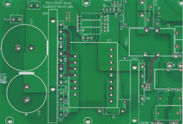
In the realm of PCB design, the importance of solder pad design cannot be overstated. While design software has made great strides, the need for comprehensive libraries catering to all types of Surface-Mounted Components (SMC) or Surface-Mounted Devices (SMD) remains. This article delves into the impact of solder pad design on Printed Circuit Assemblies (PCA) reliability and presents practical design approaches aligned with quality standards.
Rectangular Sheet-Type Component Solder Pad
When dealing with rectangular components, adherence to national and IPC standards is crucial for ensuring welding quality. The design of solder pads for such components should prioritize the solder material climbing above 1/3 of the component’s thickness on the joint’s end face, without specific requirements for the sides of the solder joint.
Solder Pad Spacing Experiment
An experiment involving 0805 components tested various pad spacings, revealing interesting insights. While a 1.8mm pad diameter offered high mounting accuracy, a 0.6mm diameter proved optimal, providing stability pre-soldering and ensuring components remained securely in place post-soldering. This balanced wetting forces on both ends, fostering reliable solder joints.
Key Findings:
- Large pad diameters (e.g., 1.8mm) increased the risk of component movement and tombstoning during soldering.
- Smaller spacing (0.6mm) enhanced component placement precision and reduced the likelihood of displacement.
Impact of Cleaning Process on Pad Spacing
Post-soldering cleaning processes play a significant role in determining optimal pad widths. When utilizing no-clean solder paste, wider pad widths can be accommodated without compromising joint strength. However, exceeding the component body width with pad width can lead to misalignment issues during placement or soldering. Aligning pad width with the component body width is advised for improved alignment and error mitigation.
Pad Length Considerations
The length of solder pads for rectangular sheet-type components directly influences solder flux availability for robust joint formation. Compliance with standards like Gtb3243-98 dictates that the soldering area’s height should exceed 1/3 of the component body thickness, necessitating adequate pad length to facilitate sufficient flux distribution.
Solder Pad Design Requirements
- Based on the previous considerations, rectangular sheet-type component pads can be designed using the methods outlined. The specific solder pad and its corresponding formula are shown in Figures 2 and 3.


Note:
- The units of measurement used are in millimeters (mm).
- If the PCB has solder pads with a pin center distance smaller than 0.5mm, the K value for designing the length of the solder pads should be maximized.
- For smaller component sizes, the spacing between solder pads should have a smaller K value in the design.
- The K values in the above formulas may vary.
If you have any inquiries about PCBs or PCBA, feel free to reach out to me at info@wellcircuits.com.