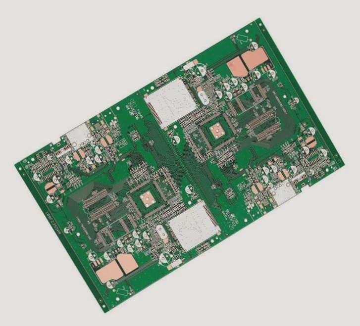
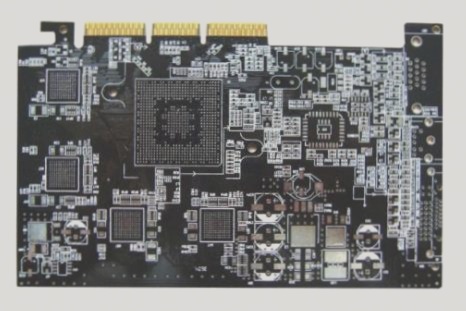
With the development of communication technology, the use of handheld wireless radio frequency PCB board technology is becoming increasingly prevalent, with applications ranging from wireless pagers to mobile phones and wireless PDAs. The performance of the radio frequency circuit directly impacts the overall product quality. One of the key features of these handheld devices is miniaturization, which leads to a high component density and increased risk of mutual interference among components, including SMDs, SMCs, and bare chips. Improper handling of electromagnetic interference signals can result in circuit failure. Therefore, preventing and mitigating electromagnetic interference and enhancing electromagnetic compatibility are critical considerations in RF circuit PCB board design. The performance of the same circuit can vary significantly based on different PCB board design structures. When utilizing Protel99 SE software for designing RF circuit PCB boards for handheld products, maximizing performance indicators is essential to meet electromagnetic compatibility requirements.
1. Selection of Substrates
Printed circuit board substrates fall into two categories: organic and inorganic. Key substrate properties include dielectric constant (εr), dissipation factor (or dielectric loss) tanδ, coefficient of thermal expansion (CET), and moisture absorption rate. Among these, εr impacts circuit impedance and signal transmission speed. For high-frequency circuits, permittivity tolerance is a critical factor to consider, with preference given to substrates with minimal permittivity tolerance.

PCB Board Design Process
Since the use of Protel99 SE software is different from that of Protel98 and other software, first, the process of PCB board design using Protel99 SE software is briefly discussed.
1) Protel99 SE adopts the project database mode management, which is implicit under Windows 99, so you should first set up a database file to manage the designed circuit schematic diagram and PCB board layout.
2) The design of the schematic diagram involves ensuring network connection by utilizing components from the component library. Any required components not found in the library should be created in SCHLIB and stored in the library file.
3) Upon completion of the schematic design, a netlist can be formed for use in PCB board design.
4) PCB board design:
a) Determine the shape and size of the PCB board based on its position in the product, space availability, and component collaboration. Utilize the PLACE TRACK command to draw the PCB outline on the MECHANICAL LAYER layer.
b) Create positioning holes, eyes, and reference points on the PCB board according to SMT requirements.
c) Produce components that are not in the library before the layout process. The process of making components in Protel99 SE is straightforward.
d) After component production, proceed with layout and wiring, which will be discussed in more detail.
e) Conduct inspection post-process completion to verify the circuit principle and overall assembly. This includes manual inspection or automated comparison between the schematic and PCB networks.
f) Once verified, archive and output the file using the “EXPORT” command in the “FILE” option.
Layout of Components
In the case of RF circuit PCB board design, the layout of components plays a crucial role in solder joint quality, electromagnetic compatibility, and overall circuit performance. It is essential to consider not only general PCB layout principles but also strategies to minimize interference and enhance anti-interference capabilities.
Wiring
Following component layout, wiring plays a crucial role in ensuring proper signal transmission and minimizing interference. Key principles include maintaining low-density wiring, consistent signal trace thickness, and strategic positioning of power and ground lines.
Conclusion
Effective design of RF circuit PCB boards involves reducing radiation and improving anti-interference capabilities. Reasonable layout and wiring strategies are crucial in achieving this goal and enhancing the reliability of PCB board designs.Implementing the described methods can help address electromagnetic interference issues and ensure electromagnetic compatibility.
1. Selection of Substrates
Printed circuit board substrates fall into two categories: organic and inorganic. Key substrate properties include dielectric constant (εr), dissipation factor (or dielectric loss) tanδ, coefficient of thermal expansion (CET), and moisture absorption rate. Among these, εr impacts circuit impedance and signal transmission speed. For high-frequency circuits, permittivity tolerance is a critical factor to consider, with preference given to substrates with minimal permittivity tolerance.

PCB Board Design Process
Since the use of Protel99 SE software is different from that of Protel98 and other software, first, the process of PCB board design using Protel99 SE software is briefly discussed.
1) Protel99 SE adopts the project database mode management, which is implicit under Windows 99, so you should first set up a database file to manage the designed circuit schematic diagram and PCB board layout.
2) The design of the schematic diagram involves ensuring network connection by utilizing components from the component library. Any required components not found in the library should be created in SCHLIB and stored in the library file.
3) Upon completion of the schematic design, a netlist can be formed for use in PCB board design.
4) PCB board design:
a) Determine the shape and size of the PCB board based on its position in the product, space availability, and component collaboration. Utilize the PLACE TRACK command to draw the PCB outline on the MECHANICAL LAYER layer.
b) Create positioning holes, eyes, and reference points on the PCB board according to SMT requirements.
c) Produce components that are not in the library before the layout process. The process of making components in Protel99 SE is straightforward.
d) After component production, proceed with layout and wiring, which will be discussed in more detail.
e) Conduct inspection post-process completion to verify the circuit principle and overall assembly. This includes manual inspection or automated comparison between the schematic and PCB networks.
f) Once verified, archive and output the file using the “EXPORT” command in the “FILE” option.
Layout of Components
In the case of RF circuit PCB board design, the layout of components plays a crucial role in solder joint quality, electromagnetic compatibility, and overall circuit performance. It is essential to consider not only general PCB layout principles but also strategies to minimize interference and enhance anti-interference capabilities.
Wiring
Following component layout, wiring plays a crucial role in ensuring proper signal transmission and minimizing interference. Key principles include maintaining low-density wiring, consistent signal trace thickness, and strategic positioning of power and ground lines.
Conclusion
Effective design of RF circuit PCB boards involves reducing radiation and improving anti-interference capabilities. Reasonable layout and wiring strategies are crucial in achieving this goal and enhancing the reliability of PCB board designs.Implementing the described methods can help address electromagnetic interference issues and ensure electromagnetic compatibility.


