Printed Circuit Boards (PCB) Fundamentals and Design Guidelines
Types of PCBs
- Single-sided PCB: Components on one side, wiring on the other.
- Double-sided PCB: Wiring on both sides connected through vias.
- Multi-layer PCB: Utilizes PTH and NPTH vias for interlayer connectivity.
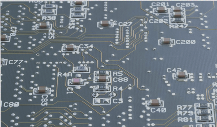
PCB Design Guidelines
- Position main components based on signal flow.
- Tackle complex circuits before simpler ones.
- Decrease component sizes from large to small.
- Segregate strong and weak signals, high and low signals, analog and digital signals.
- Keep wiring short and logical for efficient layout.
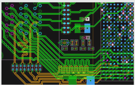
Key Design Considerations
Separate “signal ground” from “power ground” to prevent interference. Component placement should align with circuit diagrams for easier maintenance. Ground and AC wires should be wide. Minimize feedback loops and interference. Position inductive components away from heat sources.
Additional Design Tips
- Maintain distances between chips, resistors, and capacitors.
- Place input filter capacitor close to the filtered line.
- Address safety regulations, EMC, and interference by focusing on spacing, creepage, and insulation distances.
Distance Requirements
Ensure proper creepage and clearance distances for different voltage ranges. Maintain spacing between primary and secondary sides, transformer levels, and ground connections for safety.
Optimizing PCB Design
By following these guidelines and considering key factors, such as spacing and insulation distances, you can enhance the performance and reliability of your PCB designs.