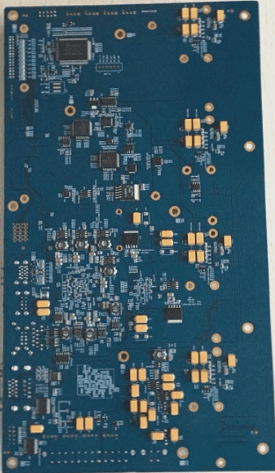
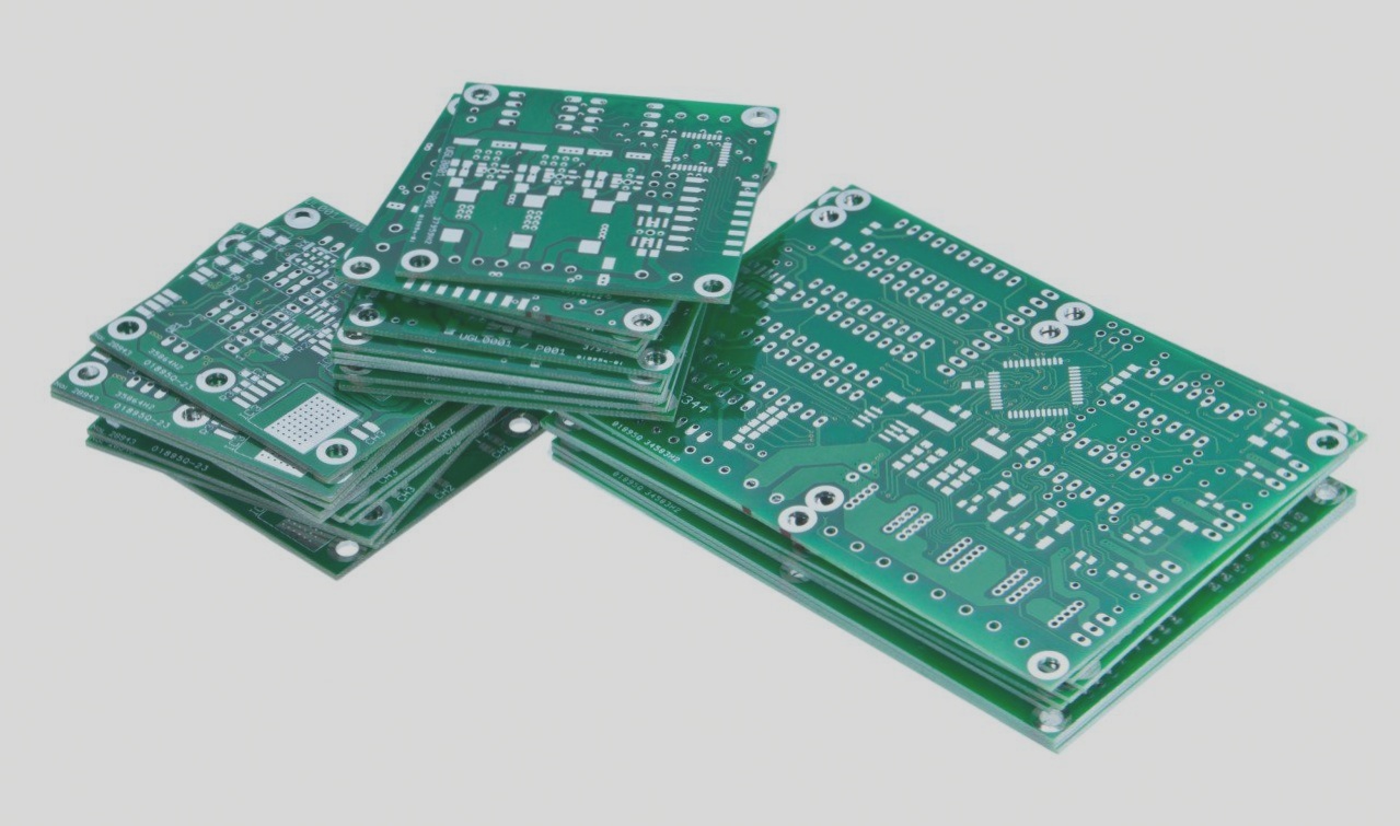
PCB multilayer boards are specialized types of printed circuit boards that serve unique purposes, such as facilitating complex circuitry. These boards are crucial for ensuring electrical components can function without interference, thereby guaranteeing safety. To achieve optimal performance from a PCB multilayer board, meticulous design is essential. Below, we outline the steps involved in designing these boards.
Design Steps for PCB Multilayer Boards:
1. Determining Board Shape, Size, and Layer Count
1.1. The shape and size of a printed board should align with the overall product structure while maintaining simplicity for efficient production. Typically, a rectangular shape with a low length-to-width ratio is preferable. This design approach enhances manufacturing efficiency and minimizes labor costs.
1.2. The number of layers in the PCB must be carefully selected based on circuit performance requirements, board dimensions, and circuit density. Commonly used configurations include four-layer and six-layer PCBs. For instance, a four-layer PCB typically consists of two signal layers (component and soldering surfaces), one power layer, and one ground layer.
1.3. Each layer of the multilayer board should be symmetrical, ideally featuring an even number of copper layers (e.g., four, six, eight layers). Symmetrical layering helps prevent board warping, which is particularly critical for surface-mounted multilayer boards and ensures reliability during operation.
These steps lay the foundation for designing effective PCB multilayer boards, ensuring they meet performance expectations while maintaining manufacturing feasibility and reliability.

2. Thin, dense wires and signal wires that are susceptible to interference are typically arranged in the inner layer. Large area copper foil should be evenly distributed in both the inner and outer layers to reduce warpage and ensure a uniform surface coating during electroplating. To prevent damage to the printed wire and interlayer short circuits during processing, the distance between the conductive pattern in the inner and outer wiring areas and the board edge should be greater than 50 mil.
3. Requirements for conductor routing and line width
For multi-layer board wiring, the power supply layer, ground layer, and signal layer should be kept separate to minimize interference. Lines on adjacent layers should be as perpendicular as possible, or take oblique lines and curves instead of parallel lines to reduce interlayer coupling and interference. Keep the wire length as short as possible, especially for small signal circuits, to minimize resistance and interference.
Avoid sharp corners when changing direction for signal lines on the same layer. The conductor width should be determined based on the current and impedance requirements of the circuit, with power input lines wider than signal lines. For digital boards, power input lines can be 50-80 mil wide, and signal lines can be 6-10 mil wide.
4. Drilling size and pad requirements for PCB multilayer boards
4.1. The size of drill holes for components on multilayer boards should be based on the pin size of the selected components. Holes that are too small can affect component assembly and soldering, while holes that are too large may result in insufficient soldering during assembly. The calculation method for element hole diameter and pad size is as follows:
4.2. Element hole diameter = element pin diameter (or diagonal) + (10-30 mil)
4.3. Component pad diameter should be equal to or greater than the component hole diameter + 18 mil. The hole diameter should be determined based on the board thickness, with the general rule that the hole diameter should be no more than 5 times the thickness of the finished board.
4.4. Via pad diameter should be equal to or greater than the via diameter + 12 mil.
This multilayer board can facilitate the conduction of various circuits and also serve as an insulating component.
Design Steps for PCB Multilayer Boards:
1. Determining Board Shape, Size, and Layer Count
1.1. The shape and size of a printed board should align with the overall product structure while maintaining simplicity for efficient production. Typically, a rectangular shape with a low length-to-width ratio is preferable. This design approach enhances manufacturing efficiency and minimizes labor costs.
1.2. The number of layers in the PCB must be carefully selected based on circuit performance requirements, board dimensions, and circuit density. Commonly used configurations include four-layer and six-layer PCBs. For instance, a four-layer PCB typically consists of two signal layers (component and soldering surfaces), one power layer, and one ground layer.
1.3. Each layer of the multilayer board should be symmetrical, ideally featuring an even number of copper layers (e.g., four, six, eight layers). Symmetrical layering helps prevent board warping, which is particularly critical for surface-mounted multilayer boards and ensures reliability during operation.
These steps lay the foundation for designing effective PCB multilayer boards, ensuring they meet performance expectations while maintaining manufacturing feasibility and reliability.

2. Thin, dense wires and signal wires that are susceptible to interference are typically arranged in the inner layer. Large area copper foil should be evenly distributed in both the inner and outer layers to reduce warpage and ensure a uniform surface coating during electroplating. To prevent damage to the printed wire and interlayer short circuits during processing, the distance between the conductive pattern in the inner and outer wiring areas and the board edge should be greater than 50 mil.
3. Requirements for conductor routing and line width
For multi-layer board wiring, the power supply layer, ground layer, and signal layer should be kept separate to minimize interference. Lines on adjacent layers should be as perpendicular as possible, or take oblique lines and curves instead of parallel lines to reduce interlayer coupling and interference. Keep the wire length as short as possible, especially for small signal circuits, to minimize resistance and interference.
Avoid sharp corners when changing direction for signal lines on the same layer. The conductor width should be determined based on the current and impedance requirements of the circuit, with power input lines wider than signal lines. For digital boards, power input lines can be 50-80 mil wide, and signal lines can be 6-10 mil wide.
4. Drilling size and pad requirements for PCB multilayer boards
4.1. The size of drill holes for components on multilayer boards should be based on the pin size of the selected components. Holes that are too small can affect component assembly and soldering, while holes that are too large may result in insufficient soldering during assembly. The calculation method for element hole diameter and pad size is as follows:
4.2. Element hole diameter = element pin diameter (or diagonal) + (10-30 mil)
4.3. Component pad diameter should be equal to or greater than the component hole diameter + 18 mil. The hole diameter should be determined based on the board thickness, with the general rule that the hole diameter should be no more than 5 times the thickness of the finished board.
4.4. Via pad diameter should be equal to or greater than the via diameter + 12 mil.
This multilayer board can facilitate the conduction of various circuits and also serve as an insulating component.


