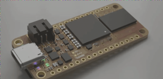
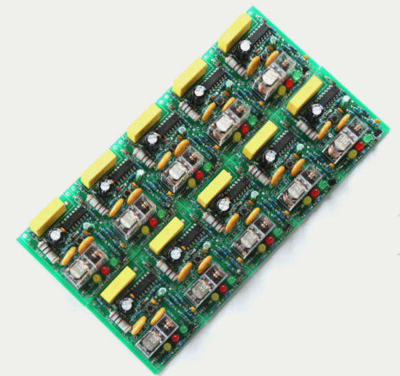
Essential Steps for Designing a High-Quality PCB for Switching Power Supplies
- 1. Schematic to PCB Design: The transition from schematic to PCB design is crucial for a successful outcome. Ensure proper component parameters, netlist creation, parameter settings, manual layout, routing, design verification, review, and CAM output.
- 2. Parameter Settings: Pay attention to trace spacing for safety and ease of production. Maintain adequate spacing for electrical stress handling, especially for high and low-level signals. Use tapered connections for thin traces connected to pads to prevent defects.
- 3. Component Layout: Proper layout is essential for optimal performance. Incorrect placement of traces can lead to delays and noise issues. Follow best design practices to avoid performance degradation.
- 4. Current Loops in Switching Power Supplies: Understand the four main current loops in a switching power supply, including power switch AC circuit, output rectifier AC circuit, input signal source current loop, and output load current loop.
- 5. Importance of Filter Capacitors: Filter capacitors play a crucial role in storing energy and filtering out unwanted components. Proper connection to the power supply through capacitor terminals is essential to prevent EMI issues.
- 6. Minimizing EMI: High-amplitude trapezoidal currents in power switch and rectifier circuits are prone to EMI. Routing these AC loops before other traces is critical to reducing electromagnetic interference.
- 7. Component Placement: Place filter capacitors, power switches, and inductive transformers close together to minimize current paths and optimize performance.

If you require PCB manufacturing services, feel free to contact us for assistance.