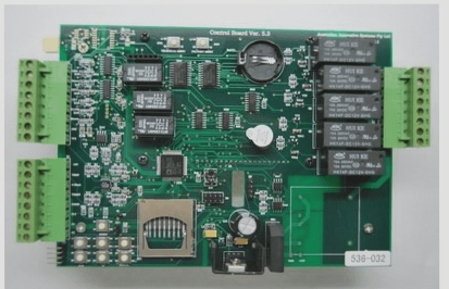
Testing is a crucial aspect of PCB board design and manufacturing. As parts continue to shrink in size, products become more complex, and time-to-market deadlines tighten, testing becomes increasingly intricate. The expanding functionality of circuit boards also raises the significance of assembly-level evaluation and on-site maintenance in the assembly process. This article presents three key strategies for designing circuit board testability.
Electronic assembly testing comprises two primary categories: bare board testing and load testing. Bare board testing is conducted post-circuit board production to verify continuity, detect short circuits, open circuits, and netlists. Additional inspection and verification methods are also utilized during this process. Load testing, on the other hand, takes place after the assembly process and is more intricate compared to bare board testing.
Tests during the assembly stage encompass production defect analysis (MDA), in-circuit testing (ICT), functional testing (to validate product performance in a real-world environment), and a combination of these approaches. Automatic optical inspection (AOI) and automatic X-ray inspection have recently been incorporated into assembly testing. They provide static and layered X-ray images of circuit boards on different planes to identify virtual soldering and solder joint bridging defects.
The goal of devising a test strategy is to create a tailored combination test plan suitable for a specific product. It is essential to define a straightforward strategy for implementing required tests early in the design process. Addressing product testability issues during the product development cycle’s early stages rather than later on can significantly reduce test costs and enhance node testability.
There are five common types of tests, each serving specific functions:
1. Bare board test: Detect open circuit and short circuit defects on the circuit board without components.
2. Production defect analysis: Identify solder joint short-circuit and open-circuit defects on the circuit board with installed components.
3. In-circuit testing: Validate the functionality of individual components.
4. Functional test: Certify the operation of functional modules in the circuit.
5. Combination test: Merge in-circuit testing and functional testing.
A well-formulated testing strategy ensures the feasibility of each conducted test. While the production test procedure may be clearly defined at the start of the development cycle, adjustments can still be made post-design completion. Adhering to a test strategy throughout the design cycle is key to achieving 100% testing of each side of the circuit board, every wiring network, and each node. The optimal test strategy depends on factors such as process feasibility, economic analysis, product lifecycle, and time-to-market requirements.
To determine the best testing approach, evaluating all inspection processes to gauge defect scope and testing costs is crucial. Identifying and resolving these issues during the design phase before product launch is essential.


