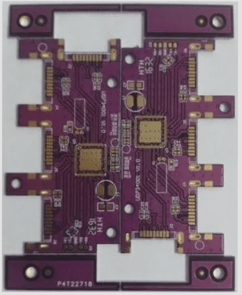
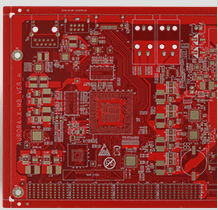
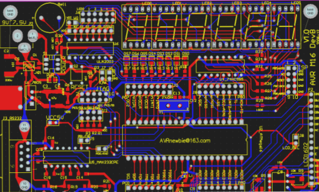
In PCB design and layout, assembly reliability, often referred to as process reliability, generally indicates the ability of a PCBA to withstand normal operations during assembly and soldering without sustaining damage. An improper design can easily lead to harm to the solder joints or components.
**How to Design for PCBA Assembly Reliability**
Devices that are sensitive to stress, such as BGAs, chip capacitors, and crystal oscillators, can be vulnerable to mechanical or thermal stress. In PCB design and layout, it’s crucial to position these components in areas of the PCB that are less prone to deformation or to implement reinforced designs or suitable measures to mitigate stress.
**How to Design for PCBA Assembly Reliability**

(1) In PCB design and layout, it’s crucial to position stress-sensitive components as far as possible from areas that are likely to bend during assembly. To prevent bending deformation during the assembly of the daughter board, the connector linking the daughter board to the mother board should ideally be located at the edge of the daughter board, with a maximum distance of 10mm from the screws. For instance, to avoid stress cracking of BGA solder joints, it’s essential to refrain from placing the BGA layout in regions susceptible to bending during PCB assembly. A poorly designed BGA can easily lead to solder joint cracks if the board is held with one hand.
How to design PCBA assembly reliability
(2) Reinforce the four corners of large-size BGAs. In PCB design and layout, the solder joints at the corners of a BGA are subjected to the highest stress when the PCB bends, making them the most vulnerable to cracking or failure. Therefore, strengthening these corners is highly effective in preventing solder joint issues. Special adhesives or patch glue should be employed for reinforcement. This approach necessitates adequate space for component placement, and the requirements and methods for reinforcement should be clearly detailed in the process documentation.
How to design PCBA assembly reliability
In PCB design and layout, the aforementioned two recommendations primarily focus on design considerations. Additionally, the assembly process should be enhanced to minimize stress generation, such as avoiding the use of supporting tools that require one-handed board handling and screw installation. Consequently, ensuring assembly reliability should not be confined to merely improving component layout. A more significant aspect involves reducing assembly stress through appropriate methods and tools, providing comprehensive training for personnel, and standardizing operational procedures. Only by addressing these factors can we effectively mitigate solder joint failure during the assembly stage.
If you have any PCB manufacturing needs, please do not hesitate to contact me.Contact me
**How to Design for PCBA Assembly Reliability**
Devices that are sensitive to stress, such as BGAs, chip capacitors, and crystal oscillators, can be vulnerable to mechanical or thermal stress. In PCB design and layout, it’s crucial to position these components in areas of the PCB that are less prone to deformation or to implement reinforced designs or suitable measures to mitigate stress.
**How to Design for PCBA Assembly Reliability**
(1) In PCB design and layout, it’s crucial to position stress-sensitive components as far as possible from areas that are likely to bend during assembly. To prevent bending deformation during the assembly of the daughter board, the connector linking the daughter board to the mother board should ideally be located at the edge of the daughter board, with a maximum distance of 10mm from the screws. For instance, to avoid stress cracking of BGA solder joints, it’s essential to refrain from placing the BGA layout in regions susceptible to bending during PCB assembly. A poorly designed BGA can easily lead to solder joint cracks if the board is held with one hand.
How to design PCBA assembly reliability
(2) Reinforce the four corners of large-size BGAs. In PCB design and layout, the solder joints at the corners of a BGA are subjected to the highest stress when the PCB bends, making them the most vulnerable to cracking or failure. Therefore, strengthening these corners is highly effective in preventing solder joint issues. Special adhesives or patch glue should be employed for reinforcement. This approach necessitates adequate space for component placement, and the requirements and methods for reinforcement should be clearly detailed in the process documentation.
How to design PCBA assembly reliability
In PCB design and layout, the aforementioned two recommendations primarily focus on design considerations. Additionally, the assembly process should be enhanced to minimize stress generation, such as avoiding the use of supporting tools that require one-handed board handling and screw installation. Consequently, ensuring assembly reliability should not be confined to merely improving component layout. A more significant aspect involves reducing assembly stress through appropriate methods and tools, providing comprehensive training for personnel, and standardizing operational procedures. Only by addressing these factors can we effectively mitigate solder joint failure during the assembly stage.
If you have any PCB manufacturing needs, please do not hesitate to contact me.Contact me

