PCB Power Supply Regulator: Everything You Need to Know
A power supply regulator is a critical component in electronic devices that automatically adjusts the output voltage to ensure stable operation. It plays a vital role in stabilizing power supply voltage fluctuations and meeting the requirements of electrical equipment.
Importance of PCB Design in Power Supply Regulators
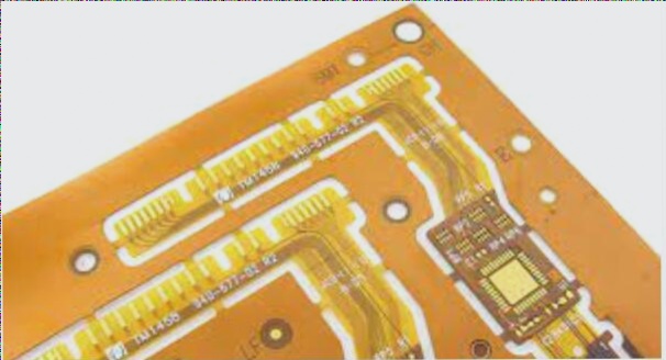
PCB design is crucial for switching power supplies, impacting performance, EMC requirements, reliability, and producibility. With advancing electronic technology, PCB layout and wiring requirements are becoming stricter. A well-planned PCB layout can significantly enhance efficiency.
Components of PCB Power Supply Regulator
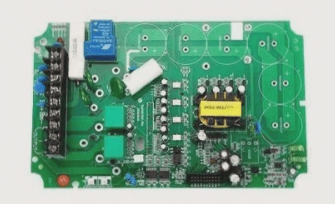
The PCB power supply regulator comprises a voltage-stabilizing circuit, control circuit, and servo motor. It automatically adjusts the output voltage by changing the position of the voltage regulator carbon brush, ensuring stability even with input voltage or load changes.
Functions of Power Supply Regulator
- Adjust output voltage
- Prevent excessive charging
- Cut off charging circuit in case of reverse current
Characteristics of PCB Power Supply Regulator
- Compact and lightweight design
- Energy-saving efficiency
- High output stability
- Modulatable output waveform
PCB Power Supply Regulator Layout Guide
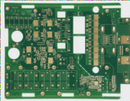
Efficient layout is crucial for power conversion, thermal behavior, EMI sensitivity, and safety in PCB power supply regulators. Maintaining low EMI, defining grounding correctly, and isolating current parts can help reduce noise coupling and ensure optimal system performance.
PCB Layout Design for Power Supply Regulators
When designing a PCB layout for power supply regulators, it is crucial to consider various factors to ensure optimal performance and reliability. Here are some key guidelines to follow:
1. Noise Management
Ensure proper noise management in the layout by using envelope tracking and EMI filter circuits when necessary. Utilize a significant amount of copper for cooling important components and consider unique shell designs, heat sinks, or fans for thermal regulation. Place fast switches and high-current circuits strategically to prevent parasitic oscillations during switching events.
2. Grounding Considerations
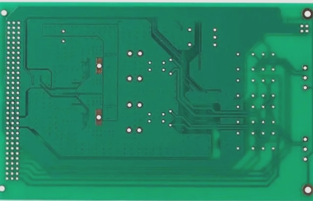
Define grounding points carefully in the layout, including input high current source ground, input high current circuit ground, output high current rectification ground, output high current load ground, and low-level control ground. Separate these grounding connections to ensure current isolation and use multiple through holes for low-impedance return paths.
3. Ground Area Design
Utilize large flat or polygonal pouring for ground areas to provide low impedance paths for noise dissipation and high return currents. Implement grounding layers on both sides to absorb radiated EMI, reduce noise, and minimize grounding loop errors. These layers also serve for electrostatic shielding and separating power and signal components.
4. Naming and Connectivity
Assign multiple names to grounding areas based on their functions and ensure correct linkage between them. Define the ground plane with low impedance connections to maintain assembly integrity and prevent interference.
In conclusion, the PCB layout design plays a critical role in the overall performance and reliability of power supply regulators. By following these guidelines, you can optimize the layout for efficient operation and reduced noise interference.