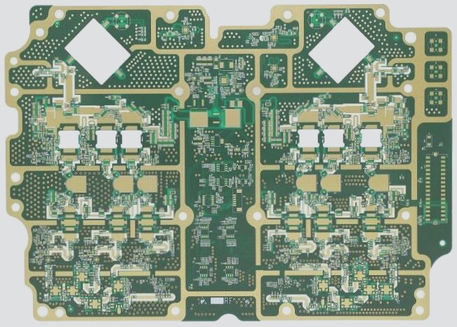
Understanding PCB Layer Placement for Optimal Electrical Behavior
Each layer in a PCB serves a specific role in determining electrical behavior. The signal plane layer is crucial for carrying power and electrical signals between components. However, positioning the copper plane correctly in the inner layer is essential for its proper functioning.
Importance of Power Supply, Grounding, and Signal Layers
In addition to the signal layer, a PCB requires power supply and ground layers placed strategically in the stack to ensure the board operates correctly.
Factors Influencing Layer Placement
The placement of power, grounding, and signal layers is a debated topic in PCB design. Designers must consider factors such as the board’s intended use, component functions, and signal tolerance.
Optimizing Signal and Plane Layers
Understanding factors like impedance variation limits, jitter, voltage ripple, PDN impedance, and crosstalk suppression helps in arranging signal and plane layers effectively on the board.

Choosing the Right Number of Signal Plane Layers
When determining the required number of signal plane layers, consider the number of signal networks, signal width, and spacing. Follow steps to estimate the number of signal layers needed based on the net count and board size.
Designing PCB Lamination for Optimal Performance
Arrange PCB layers symmetrically to prevent warping during assembly. Design plane and signal layers carefully for impedance-controlled wiring to ensure optimal performance.
Implementing Controlled Impedance Wiring
Utilize strip line impedance equations to design ribbon lines and microstrip lines for controlled impedance wiring between planar layers. Consider geometric parameters and layer thickness for impedance control.
PCB Design Considerations for Impedance Control and Signal Integrity
When designing PCBs, it is crucial to consider impedance control and signal integrity to ensure proper functionality of the circuit. Here are some key points to keep in mind:
Microstrip Lines and Impedance Calculations
- For microstrip lines on the surface layer, determining the layer thickness, copper weight, and line width is essential to define the characteristic impedance.
- PCB design tools offer impedance calculators to help determine the optimal wiring size for achieving the desired characteristic impedance.
- For differential pairs, defining the lines as a pair in each layer allows the impedance calculator to determine the correct spacing between the lines.
Impedance Analysis and Adjustment
- During board wiring, traces may be coupled to other traces and conductors, leading to impedance variations.
- Use impedance analysis tools to monitor impedance across the signal network and make adjustments to meet impedance targets.
- Impedance changes along traces can be highlighted in red, prompting adjustments in trace spacing to eliminate variations.
Signal Integrity for Analog and Mixed-Signal Boards
- For analog boards, power integrity is straightforward, but signal integrity can be challenging.
- For mixed-signal boards, combine digital and analog approaches to ensure both signal and power integrity.
Signal Isolation and Return Path Planning
- Grounded copper pours or fencing can be used to isolate different parts of the board and create coplanar waveguides for high-frequency analog signals.
- Proper return path planning is crucial when mixing analog and digital signals to prevent interference.
- Separating digital and analog signals into different layers with dedicated ground layers helps maintain isolation.
Power Supply Considerations
- For analog components connected to AC power, a dedicated analog power board may be necessary to manage return path planning.
- Separate switching noise from DC and AC parts to prevent interference between different power and grounding sections.
By following these guidelines and utilizing advanced PCB design tools, engineers can optimize impedance control and ensure signal integrity in their circuit designs.


