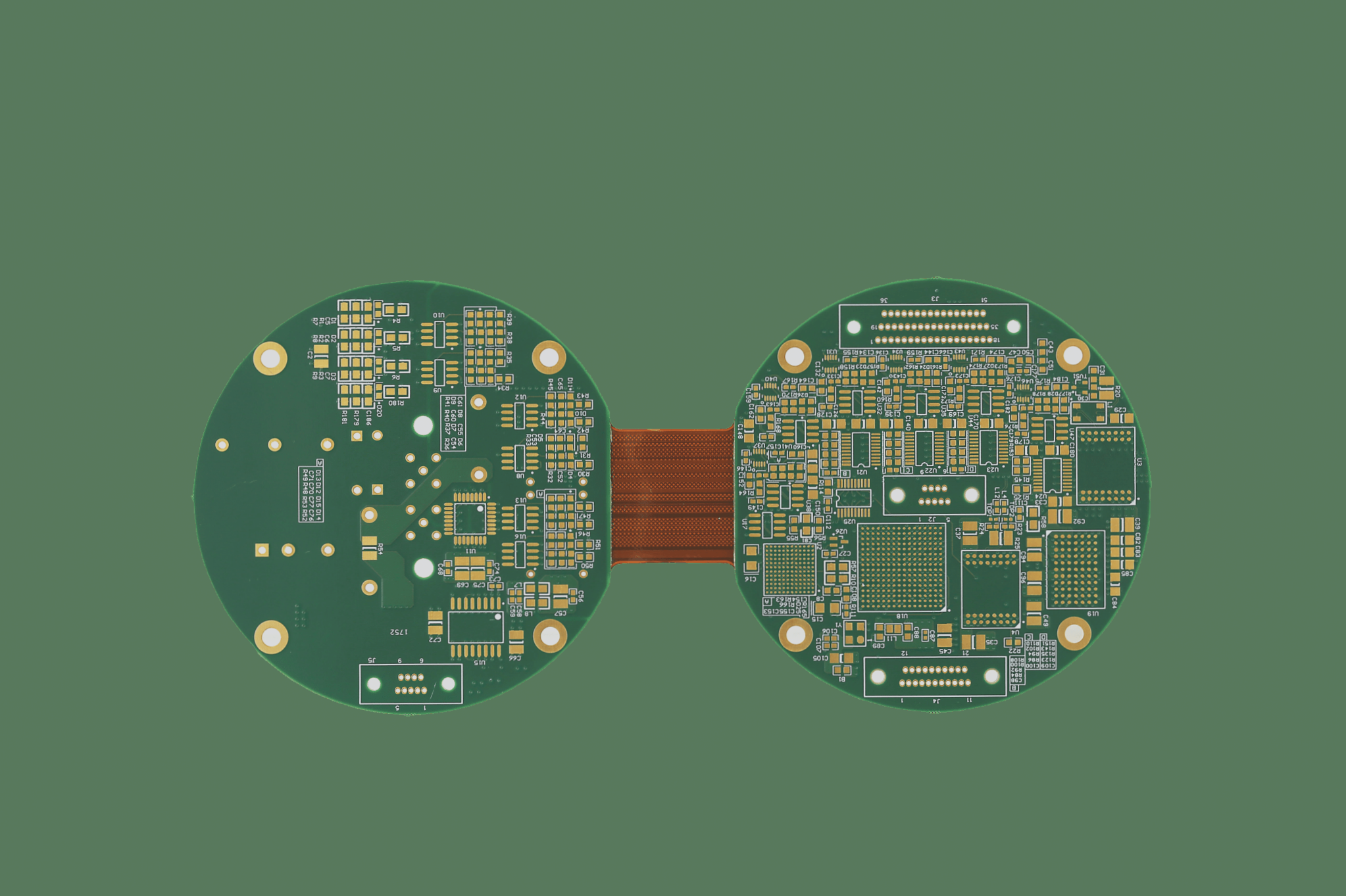
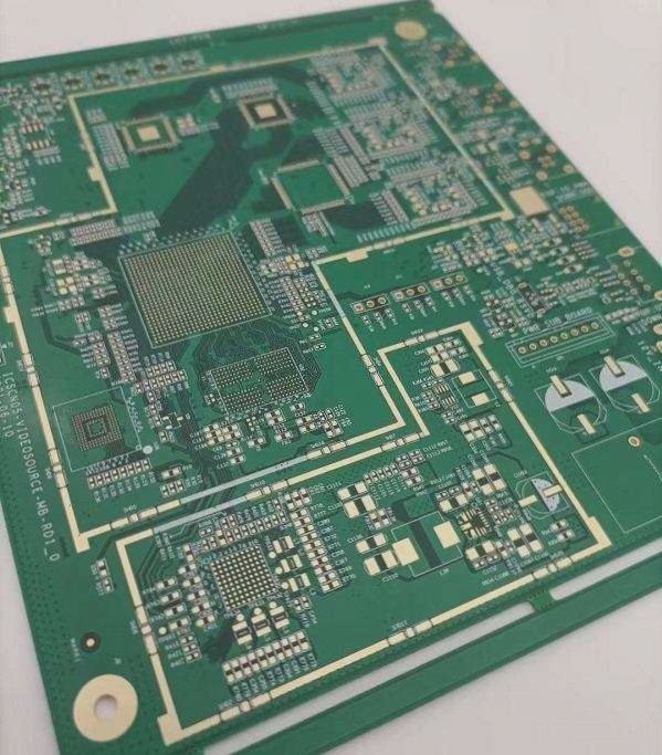
Enhancing PCB Manufacturing Efficiency with Design for Manufacturability (DFM)
Typesetting and Layout Tips:
- Opt for board sizes below 23cm × 30cm to ease production transportation and stability.
- Keep board sizes uniform to minimize downtime and solder temperature profile variations.
- Integrate panels only for products with identical production requirements.
- Route wiring predominantly on the top surface to prevent damage during production.
- Use oval pads for high-pin count components to avoid solder bridges.
- Maximize spacing between positioning holes and components for easier insertion.
- Utilize positioning holes as PCB mounting holes to reduce drilling during production.
- Include a test circuit pattern for process control on the waste side of the board.
- Leave a central passage for larger boards during wave soldering to ensure consistent soldering.
- Design for testability by considering needle bed layout and using flat pads for better testing connections.
Positioning and Component Placement Recommendations:
- Arrange components in rows and columns following a grid pattern to avoid board rotation during insertion.
- Group similar elements uniformly and orient components consistently for faster insertion and error detection.
- Place dual in-line package devices perpendicular to wave soldering direction to minimize solder bridging.
- Utilize silk screen printing to streamline manufacturing processes and aid in component identification.
- Include visible component reference designators and polarity markings for inspection and maintenance.
- Maintain a minimum distance between components and board edges for easier handling.
- Elevate components above the board surface with spacers to prevent mechanical damage.
By implementing these DFM strategies, you can enhance the efficiency, reliability, and competitiveness of your PCB manufacturing process.
Avoiding Assembly Complexities in PCB Design
- Minimize assembly complexity by avoiding components on both sides of the PCB.
- Cluster bottom-side components closely for easier solder mask application.
Optimizing Component Placement
- Distribute components evenly to prevent warping and ensure uniform heat distribution.
Machine Insertion Best Practices
- Standardize pad dimensions for optimal machine insertion performance.
- Select components suitable for machine insertion based on equipment specifications.
- Prefer axial components for lower insertion costs.
- Strategically place radial components to minimize assembly challenges.
- Convert component types to streamline insertion processes.
Effective Wire and Connector Strategies
- Use connectors instead of direct wire connections.
- Employ wires of different colors to prevent errors.
- Design connectors with larger pads for robust connections.
- Minimize use of dual-in-line package sockets for reliability.
- Engrave directional marks on connectors for correct installation.
Designing for Efficiency
- Select components early to align with DFM principles.
- Avoid components that require excessive force to prevent PCB damage.
- Rationalize component diversity for simplified procurement.
- Design boards with versatility for field adjustments.
General Requirements for PCB Design
- Specify areas where conformal coating is unnecessary to avoid issues.
- Optimize through-hole design for ease of insertion and soldering.
- Source components per industry standards to streamline production.
- Standardize lead wire lengths for improved soldering performance.
- Avoid slow installation methods for efficiency.
Enhancing Efficiency with DFM
Design for Manufacturability (DFM) principles improve efficiency and cost-effectiveness in PCB assembly, reducing engineering changes and design compromises.