PCB Manufacturing Process Optimization
SMT Process Advantages
- Small size, light weight, and excellent interconnectivity
- Improved performance and reduced parasitic impedance for high-frequency circuits
- Good shock and vibration resistance
- Enhanced signal-to-noise ratio by preventing signal interference
Recent studies show that optimizing solder joint formation is crucial for the success of the SMT process. Adequately designed pad sizes and component density play a significant role in ensuring the effectiveness of the PCB board.
PCB Board Material Selection
When selecting materials for PCB boards, factors such as thermal conductivity, heat resistance, solderability, and electrical conductivity need to be considered. The choice of substrates, such as FR-4, can impact the performance and reliability of the circuit board during surface mount assembly.
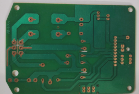
PCB Board Via Holes and Component Layout
Via Layout
- Avoid placing vias within or less than 0.6mm of the surface mount pad
- Ensure appropriate gap between via hole diameter and component lead diameter
- Avoid connecting vias and pads to prevent solder loss
Component Layout
- Components should be evenly distributed for uniform heat and space distribution
- Align components in the same direction to reduce welding issues
- Maintain a spacing of at least 0.5mm between components
Component Orientation
- Arrange passive components parallel to each other
- Align passive components and SOIC axes perpendicular to each other
- Consider adaptability of component pins and weight during assembly processes
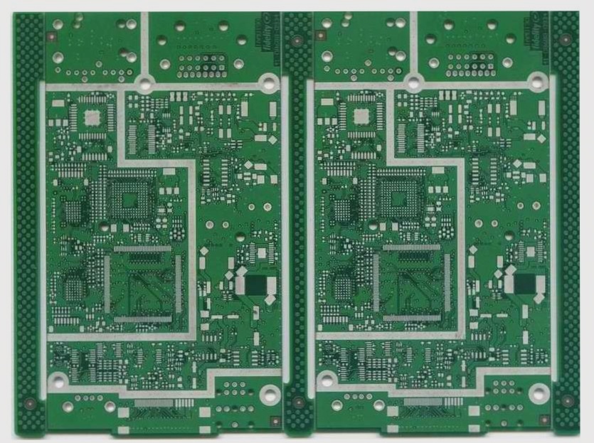
PCB Circuit and Pad Design
Proper circuit process design, including maintaining a clamping edge of 5mm in the PCB process, is essential for ensuring the reliability and functionality of the printed circuit board.
Circuit Board Design Best Practices
- Avoid connecting wires to pads at angles; connect wires perpendicular to component pads.
- Reduce wire connection width to around 0.4mm or half the pad width for better heat dissipation and solder flow control.
- Adjust trace width and spacing based on etching technology and assembly method.
- Avoid interconnection lines passing through adjacent pads.
- Consider different lead widths for various assembly methods.
- Avoid short connections between pin pads of multi-pin components.
- Ground square-shaped pads of bare chips and plate evenly with gold for reliable bonding.
Circuit Electrical Design Tips
- Follow wire-passing principles within pin spacing for different density requirements.
- Maintain consistent line width for impedance matching.
- Use short lines for small signal circuits to reduce resistance and interference.
- Separate power, ground, and signal layers to minimize interference.
- Design adjacent large-area power and ground layers to act as a capacitor for filtering.
Pad Design Guidelines
- Design pads according to specific component specifications to ensure reliability.
- Base pad size on component package shape, pins, and special requirements.
- Adhere to industry standards like IPC-SM-782, IPC-7095 for common pad designs.
- Consider symmetry, size calculations, and solder joint reliability during pad design.
- Design pads to prevent non-wetting joints and ensure good soldering.
- Ensure thermal isolation for pads connected to large conductive areas and provide dummy pads for wave soldering.
Fiducial Mark Production Requirements
- Use square, circle, triangle, or cross shapes for datum marks with a diameter of 0.5mm to 3mm.
- Maintain consistent mark size on the same board, at least 5mm away from the board edge.
- Use bare copper or plated marks with specified thickness and surface flatness.
- Ensure symmetry and space around reference point marks for accurate alignment.
- Utilize stamp plate or V-groove separation technology for jigsaw PCBs to enhance equipment utilization.