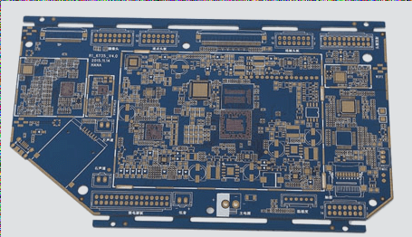
PCB Board Path Detection Circuit
The PCB board path detection circuit is designed to achieve three main functions:
- Automatic selection and measurement of the “pin pairs” to be tested
- Automatic determination of the path relationship between “pin pairs”
- Automatic recording of the measurement results
Automatic Selection and Measurement of Tested Pin Pairs
To enable the detection circuit to select different pins for measurement, a switch array is utilized. The program controls the on/off state of different switches to direct the component pins into the measurement channel. An analog multiplexer is used to form the switch array.
Measurement of On/Off Relationship
The open/closed status of the analog multiplex switch is controlled by the program through a decoding circuit. This allows for the measurement of the on/off relationship between all pins connected to the measuring head based on the combination principle.
Judgment of Pathway Relationship
Threshold voltage is proposed to determine the path relationship between measuring heads. A voltage comparator compares the measured voltage against the voltage drop on the analog multiplexer’s on-resistance. The threshold voltage value is experimentally determined, and a dynamic setting of the threshold voltage is implemented based on measured values.
Special Cases of Measurement Results
Special cases such as the influence of capacitance and inductance are considered in the measurement results. Capacitors bridging tested pins can lead to false path readings, which can be addressed by increasing the measurement current or implementing software verification.
Understanding Inductance and Capacitance Measurements in PCB Fabrication
- Inductance is often perceived as an open circuit due to its high static resistance impedance. Despite this, modern detection circuits can accurately identify the electromotive force induced by inductance, offering a contrast to capacitance measurements.
- Effects of Analog Switch Jitter:
- Analog switches may experience voltage fluctuations during the transition from open to closed states, necessitating the verification of consistent initial measurements.
- Confirmation and Recording of Measurement Results:
- To tackle these challenges, a software block diagram is employed to confirm and log measurement outcomes. This approach extends the measurement duration to mitigate capacitive influences, integrating induced electromotive force for inductance identification. Two counters, passage count (N) and open circuit count (n), are utilized to eliminate erroneous readings caused by capacitor charging and analog switch jitter. The optimal counter values and delays are determined through experimental assessment to address conflicting measurement scenarios. Software validations ensure precise path determination despite potential inaccuracies.
- This study presents an innovative method for evaluating the interconnections between component pins on extensive PCB boards. It delves into the operational and implementation principles of PCB board path detection circuits, showcasing their efficiency, accuracy, and comprehensive measurement and recording functionalities through supporting measurement and navigation software.
This revision aims to enhance the clarity, consistency, and technical precision of the original content while preserving its core message and improving readability and coherence.