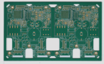
Creating a Low EMI Prototype: Essential Steps for Success
- Design circuits with low radiation to reduce electromagnetic interference (EMI).
- Perform pre-compatibility testing using 3D electromagnetic field simulation software.
- Utilize a spectrum analyzer for near-field electromagnetic scanning of the prototype PCB.
- Verify EMI performance in a microwave anechoic chamber test.
Designing for Low EMI Circuitry
Minimize radiated emissions by integrating ferrite beads and decoupling capacitors into the circuit design. These components help filter out EMI and reduce noise ripple from digital loads, lowering the risk of EMI generation.
PCB Layout Considerations for High-Frequency Signals
Ensure PCB traces follow a continuous loop, referencing the ground plane to minimize EMI. Avoid signal paths passing through dividing planes and holes to prevent unwanted radiation paths. Place ground vias next to signal vias for a proper return path, reducing the chance of erratic current flow and unintended EMI sources.

Effective PCB Design Strategies
Implement a robust grounding scheme and separate ground planes for different circuit types to minimize EMI. Conduct simulations before manufacturing to assess EMI risks and ensure compliance with standards. Perform near-field electromagnetic scans to evaluate EMI performance and boost designer confidence in meeting required standards.
EMI Simulation and Analysis
After PCB layout design, use EMI simulation tools like EMPro 2013.07 to model the electromagnetic field. Select differential signals for simulation using the Finite Element Method (FEM) to evaluate electromagnetic behavior and ensure optimal EMI performance.
Guidelines for Accurate PCB Simulation
- The boundary size should be at least eight times the PCB thickness.
- The grid size should not exceed 1/5 of the PCB width.
- A powerful computer system with over 16GB of RAM and 100GB of storage is required for efficient analysis.
EMI Simulation Process
During the simulation, a far-field sensor captures the emitted electromagnetic field. Using EMPro’s EMI simulation template, the far-field emission power is calculated, and a frequency-domain response graph is generated at a 10-meter distance with an electric field probe. Results are cross-checked with the Finite Difference Time Domain (FDTD) method.
Radiation Power Levels and Compliance
A typical simulation may show radiation levels below the FCC’s maximum threshold of 45 dBμV. Peak power intensity at 400 MHz, measured at -66.4 dBm, can be identified using a spectrum analyzer with a 30 kHz resolution bandwidth. To pass the far-field EMI compliance test, peak power should stay below -65 dBm at distances of 3 meters and 10 meters, following CISPR 11 Class A standards.
Benefits of Low-EMI Circuit Design and Testing
Implementing low-EMI design techniques and pre-compatibility testing like 3D simulations can prevent PCB redesigns, saving time and costs. This approach streamlines EMI compliance testing, ensuring timely market entry.
Common PCB Surface Coating Options
- Electrolytic Nickel/Gold (Ni/Au): Stable and durable with higher cost.
- Immersion Silver (Immersion AG): Less costly but prone to issues like electromigration.
- Electroless Nickel/Immersion Gold (ENIG): Popular but may have stability concerns.
- Electroless Tin (Lead-free Immersion Tin): Maturing and reliability may vary.
- Hot Air Solder Leveling (HASL): Evolving process with consistency challenges.
- Organic Solderability Preservatives (OSP): Cost-effective but offers lower performance.
Conclusion
Ensuring low EMI in PCB design involves strategic grounding, thorough simulation, and careful coating selection. Following best practices in EMI analysis and using suitable coatings can enhance performance, reliability, and regulatory compliance, avoiding costly redesigns and reducing development time.


