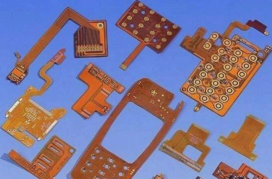
Essential Elements of PCB Anti-Interference Design
In the realm of electronic system PCB design, it is crucial to consider and address anti-interference requirements from the outset to save time and avoid potential issues post-design. Interference in PCB design typically stems from three primary elements:
- Interference Source: This pertains to components, equipment, or signals that produce interference, often represented mathematically as du/dt. High di/dt areas, such as lightning, relays, thyristors, motors, and high-frequency clocks, serve as common sources of interference.
- Propagation Path: The path or medium through which interference travels from its source to sensitive devices. Conduction through wires and radiation from the environment are typical propagation paths.
- Sensitive Devices: Devices easily disrupted by interference, including A/D and D/A converters, microcontrollers, digital ICs, and weak signal amplifiers.
The core tenets of anti-interference PCB design involve suppressing interference sources, eliminating propagation paths, and bolstering the anti-interference capabilities of sensitive devices. This strategy parallels preventive measures against infectious diseases.
If you are looking for further guidance or adjustments, feel free to reach out!