The Future of PCB Design: Multi-Board Systems
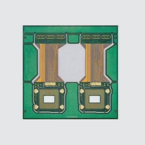
In the field of electronics, collaboration and system development have traditionally been done in isolation. However, the introduction of PCB board system-level multi-board design is revolutionizing the industry.
Benefits of Multi-Board Schematic Design
- Streamlined Process: CAD tools now support the development of multi-layer ECAD schematic systems, eliminating the slow and costly traditional methods.
- Enhanced Connectivity: Each board in the system schematic allows for continuity checks and validates inter-board connections without physical prototyping.
- Efficiency and Cost-Effectiveness: The multi-board development process ensures alignment with the overall system, reducing prototyping needs and production costs.
- Real-Time Visibility: Designers can see how different parts work together, accelerating the creation of schematics and layouts.
Design Tips for Multi-Board Systems
- Think Big Picture: Organize data collectively to reduce workload and manage system-level functionality efficiently.
- Collaboration is Key: Develop system design libraries collectively, standardize design rules, and maintain documentation for streamlined processes.
- Finalize with Care: Clean up designs, add necessary labels, and perform thorough checks to ensure all details meet company standards.
- Utilize Design Tools: Ensure your tools support complete system schematic design, simulation, 3D PCB layout display, and ECAD/MCAD collaborative design.
Conclusion
Embracing multi-board schematic design not only improves efficiency and cost-effectiveness but also enhances connectivity and collaboration in PCB development. By following best practices and utilizing advanced design tools, engineers can create complex systems with ease and accuracy.
Explore More:
Discover the latest trends in PCB fabrication and design at Well Circuits.


