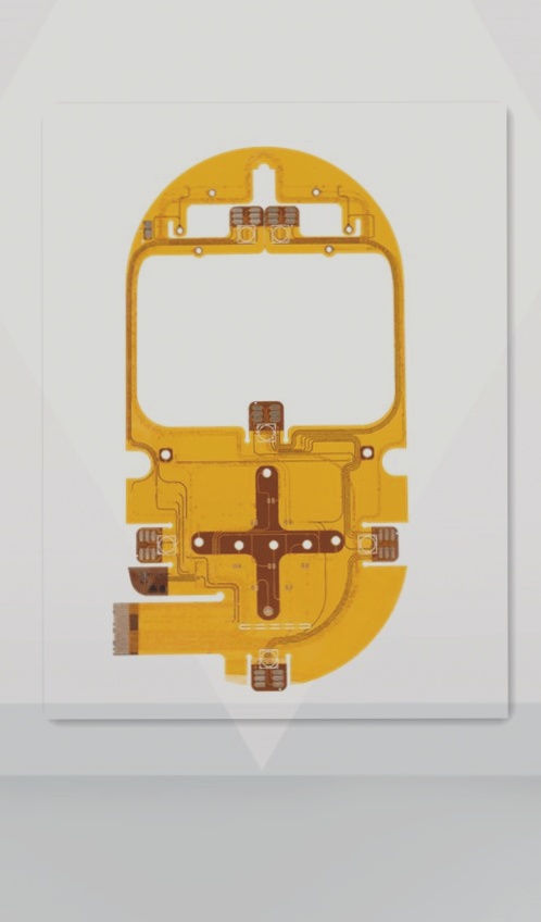
PCB Board Layout Designers and Layer Stackup Planning
PCB board layout designers typically do not directly plan the layer stackup for the circuit boards they design. While they need to know the number of layers and their configuration, they are not extensively involved beyond that. This is mainly due to historical performance requirements, limited materials, and less advanced design tools.
Evolution of PCB Layer Configuration
Fortunately, modern design tools now offer advanced PCB layer configuration capabilities, allowing designers to configure the correct layer stack-up for their designs. With the increasing complexity of circuit demands and component counts, designers face challenges in achieving desired electrical performance while balancing manufacturing costs.
Adapting to Advanced Electronics
As board functionality evolves, higher operating speeds and specialized applications may require more advanced fabrication materials, impacting the transmission line properties and layer stacking configurations. Designers must ensure the correct board layer stackup to maintain high performance standards.
Challenges Faced by Layout Designers
Layout designers encounter various challenges, including the need for quick product development, complex layer configurations, and unfamiliar materials. Some designers may require external assistance due to the complexity of the processes involved.
Assistance from PCB Design Tools
PCB CAD tools offer features such as automatic generators and wizards to streamline the creation process of board layer stackups. Designers have full control over details like conductive and dielectric materials, allowing for precise configuration and layout parameters.

Importance of Industry Knowledge in PCB Design
While PCB design tools are essential for designers, industry knowledge plays a crucial role in creating successful circuit board designs. Designers need to understand the materials and processes involved in PCB manufacturing to optimize their designs effectively.
Collaboration with PCB Contract Manufacturers
One valuable source of industry knowledge is collaborating with PCB contract manufacturers. These manufacturers have extensive experience in PCB production and can offer valuable insights into creating board layer stackups.
Early Engagement for Optimal Results
It is recommended that layout designers engage with PCB contract manufacturers early in the design process. By consulting manufacturers before starting the PCB design, designers can ensure the correct lay-up and enhance the overall quality of the circuit board.