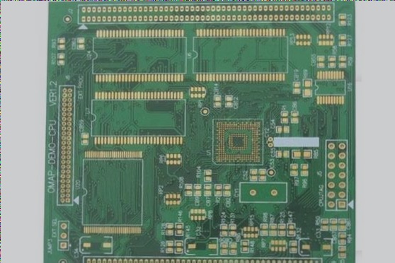
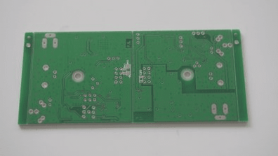
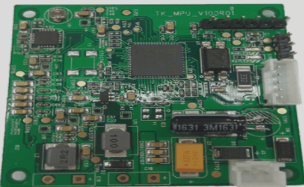
In PCB circuit board design, one common issue faced by customers and design engineers is the confusion between “via cap oil” and “via opening window” when placing orders in the system. Specifically, the distinction between Vias and Pads is often unclear, leading to uncertainty about which option to choose. This article aims to clarify these concepts and provide guidance on how to approach these decisions.

### The Problem of Non-Standard Designs

In my experience, one of the most frequent challenges is the lack of standardization in PCB designs. This often results in difficulty distinguishing between the pad and via, causing confusion in the design and manufacturing process. For example, sometimes the conductive hole is treated as a pad, and other times, the keyhole is treated as a via. This inconsistency in how VIA and PAD attributes are assigned can lead to incorrect processing and significant production delays.

### The Role of PAD and VIA Attributes

The key to resolving this issue lies in understanding the proper attributes for PADs and VIAs. A PAD is typically a copper surface area where components are soldered, while a VIA is a hole that connects different layers of the PCB. However, the problem arises when these attributes are used interchangeably or incorrectly assigned, such as using VIA attributes for pads or vice versa.

When VIA attributes are used for pads, it can cause errors during manufacturing, as the system may misinterpret the required process for pad and via holes. Similarly, improper treatment of vias as pads can result in misalignment during the lamination and drilling stages.

### The Impact on Production

For PCB manufacturing plants, handling CAM (Computer-Aided Manufacturing) data becomes more complicated when the design documents are not standardized. CAM engineers often need to revise the customer’s design files to correct inconsistencies in VIA and PAD attributes. These revisions are typically based on the engineer’s experience, which can lead to further delays or mistakes if not done properly.

The lack of clear distinction between VIA and PAD attributes can also affect other aspects of the PCB manufacturing process, such as layer stacking, hole drilling, and final inspection. This makes it crucial for customers and designers to adhere to proper design standards to minimize errors and improve efficiency.

### Conclusion: Best Practices for Avoiding Confusion

To avoid these common issues, it is essential for PCB designers to follow standardized practices when defining VIA and PAD attributes. Clear documentation and adherence to design guidelines will ensure that CAM engineers can process the data correctly without needing to make significant revisions. Additionally, when placing orders, customers should carefully review their design files and verify that the appropriate VIA or PAD options have been selected.

By maintaining a consistent and standardized approach to design and manufacturing, both engineers and customers can avoid costly mistakes and ensure a smoother PCB production process.

**PCB Design and File Preparation Best Practices: A Guide to Conductive Holes, Keyholes, and File Integrity**

Inconsistent design practices have led to several issues with customer projects. This article aims to address common pitfalls related to PCB design, focusing on conductive holes, keyholes, and the interaction between Protel, PADS, and Gerber files. It will provide guidance to ensure that your designs meet the required standards and reduce common disputes with manufacturers.

### 1. **Adhering to Design Standards and Specifications**

It is crucial for engineers to follow design standards and specifications to avoid errors. The mistakes made in previous designs often stem from not adhering to these standards. As a general rule, **do not rely on assumed “experience”**; instead, work directly according to established design guidelines. Ensuring that customer documents remain as close to their original state as possible will help minimize issues during production. This approach not only improves design quality but also reduces the likelihood of problems during manufacturing.

### 2. **Key Design Elements: Conductive Holes, Keyholes, and Pads**

There are specific design elements that require careful attention, such as **conductive holes, keyholes**, and **pads**. The following points highlight the most common issues:

#### 2.1 **Pads and Vias: A Common Mixing Issue**

One of the most frequent issues arises when **pads** and **vias** are incorrectly mixed in the design. When sending files to the manufacturer, it’s important to check whether a **via** hole is mistakenly treated as a **pad** (or vice versa). This can lead to problems when applying solder mask or covering vias with “via hole cover oil.”

**Key Tip:** When working with **pads or Protel files**, always verify that the via hole does not share the same attributes as a pad. If it’s a **pad** for a through-hole component, it should not have a via applied to it.

#### 2.2 **Via Cover Oil: Avoiding Disputes**

Another issue occurs when via holes need to be covered with **cover oil**, but the file contains both vias and pads. In some cases, a **pad** (often for through-hole components) is mistakenly marked as a via, causing the system to incorrectly apply via cover oil, which results in issues such as poor solderability.

**Common Dispute:** A customer may ask why a **via** has been “covered with oil” or why a **window** has been opened. To prevent this, always ensure that the design and Gerber files are accurate and match the intended configuration.

**Tip for Engineers:** Double-check if the via is truly intended to be a **via** or a **pad**. Vias and pads should not be mixed in the same context.

### 3. **Protel and PADS: Key Considerations for Via and Pad Design**

When working with Protel or PADS, it’s important to understand the specific functions of each component:

– **Via (in Protel or PADS):** A via is used to establish electrical connections between different layers of the PCB. Ensure that vias are correctly designated and are not confused with pads, which are used for component leads.

– **Pad (in Protel or PADS):** Pads are used for through-hole or surface-mount components. They should never be treated as vias. Confusion between these components can lead to improper manufacturing outcomes.

**Protel and PADS Tip:** When creating a **via**, ensure that you follow standard rules for via design, and if using **pads**, treat them correctly as component leads.

### 4. **Understanding the Gerber Files and Solder Mask Layers**

During file transfer to the manufacturer, discrepancies in Gerber files can cause confusion. Specifically, the solder mask layer plays a critical role in determining whether a via or a pad is covered with solder mask or oil.

– **Gerber Files and Solder Mask:** In Gerber files, **solder mask layers** control how the solder mask will be applied to the PCB. **If the solder mask is not checked** for vias, the vias will be **capped**, potentially causing problems during soldering.

– **Window Opening for Vias:** If a solder mask is incorrectly applied, it could result in unintended **window openings**. This can lead to soldering issues, such as short circuits or poor solder joint integrity.

**Reminder:** Always check if the solder mask layer is correctly defined in the Gerber files before sending them for production. This will ensure that vias are correctly capped or exposed based on design needs.

### 5. **The Importance of Proper File Conversion and Standard Practices**

When converting files between Protel, PADS, and Gerber formats, it’s essential to maintain clarity in how **vias** and **pads** are represented. Many issues arise during the **via conversion process** due to non-standard PCB design practices or unclear Gerber settings.

**Common Issue:** The factory may be unable to distinguish between a **via** and a **keyhole** (pad hole) based solely on Gerber files. If the solder mask layer isn’t properly indicated, vias may be wrongly capped or left open, causing production delays or faults.

**Best Practice:** Always ensure that your design files are standardized and clearly indicate whether you’re designing a **via** or a **pad**. If the file is unclear, the manufacturer will default to processing based on what’s provided, potentially resulting in unwanted errors.

### 6. **Conclusion: Standardized Practices Lead to Fewer Issues**

The key takeaway from this article is simple: **design with clarity** and adhere to industry standards. Whether you’re designing **vias**, **pads**, or **conductive holes**, always follow the appropriate rules for each component. Consistency across your design files—especially in the **Gerber files**—is essential for a smooth handoff to manufacturers. By using standard practices and ensuring proper file checks, you can avoid the common issues that arise in PCB design and manufacturing.

Remember, when designing for **vias**, ensure correct application of cover oil. When working with **pads**, treat them as through-hole component connections. By maintaining these standards, you will ensure a more efficient manufacturing process with fewer disputes and improved product quality.

If you have any questions about PCB or PCBA, feel free to reach out to me at info@wellcircuits.com.

Please enable JavaScript in your browser to complete this form.

Quick Quote

Info
Click or drag a file to this area to upload.
send me gerber or pcb file,format:7z,rar,zip,pdf

Contact

WellCircuits
More than PCB

Upload your GerberFile(7z,rar,zip)