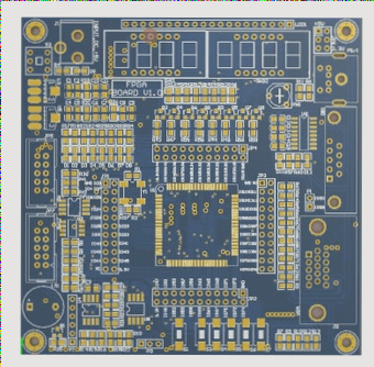
HDI Boards and Advanced Via Technologies
HDI (High-Density Interconnect) boards are essential components in today’s high-end electronic devices. These PCBs offer superior design capabilities, allowing for more compact and efficient circuit layouts compared to traditional boards. By incorporating advanced techniques like microvias, fine traces, and high-density interconnections, HDI boards enable the creation of smaller, faster, and more reliable electronic products.
Blind Vias in PCB Design
Blind vias are crucial elements in maximizing PCB density and efficiency. These vias connect inner layer traces to the outer surface without traversing the entire board thickness. By utilizing the inner layers effectively, blind vias increase density while preserving surface area for additional components.
Buried Vias for Space Optimization
On the other hand, buried vias connect traces exclusively between inner PCB layers, remaining hidden from the board’s exterior. These vias optimize space and are commonly employed in complex, high-performance HDI designs to enhance functionality and miniaturization.
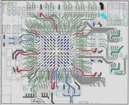
Blind and Buried Via Technology in HDI Boards
Blind and buried vias are integral to the design of HDI boards, especially in modern portable devices with demanding requirements. These advanced via technologies enable the creation of high-performance, compact, and reliable circuit boards essential for today’s electronics.
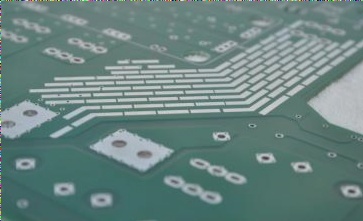
Key Design Considerations for PCBs
- Avoid Large Pads Between SMD Components: To prevent misalignment during reflow, it’s advisable to steer clear of large pads between surface mount device (SMD) components. Opt for smaller pads and thinner wires for better component placement and alignment.
PCB Design Best Practices for Optimal Manufacturing
When designing a PCB, it is crucial to consider various factors to ensure optimal manufacturing and functionality. Here are some key best practices to keep in mind:
1. Avoid Through-Holes Near Pads
Minimize the placement of through-holes near component pads to prevent soldering issues such as insufficient soldering, solder bridges, and short circuits. These problems can lead to reliability issues and manufacturing defects.
2. Pin Spacing and Jumper Placement
Reduce the pin spacing between axial devices and jumpers to streamline the assembly process and minimize the chances of errors. This optimization enhances assembly efficiency and reduces the need for adjustments.
3. Utilize Advanced Techniques
As PCB designs evolve to meet the demands of smaller and more powerful devices, consider using advanced techniques like blind and buried vias for high-density interconnects. These methods offer compact and reliable solutions for intricate designs.
4. Wave Soldering Considerations
For wave soldering processes, ensure proper solder resist between chip IC pads and incorporate “tin-stealing” pads on final legs to prevent solder bridging. Attention to these details can improve soldering quality.
5. Component Alignment and Pad Design
Match component hole shapes, pad designs, and component leads precisely for standard PCB designs. Symmetrical pads around the hole center promote proper solder joint formation, ensuring full coverage and reliable connections.
6. Soldering Oven Preparation
Position solder pads away from the tinning area for components soldered after passing through a soldering oven. Optimal orientation and hole diameter between 0.5mm and 1.0mm help prevent defects during the soldering process.
7. Enhance Mechanical Strength
Increase copper thickness around pads to bolster the mechanical strength of side leads. This enhancement aids in self-centering during reflow soldering, leading to more consistent and reliable solder joints.