
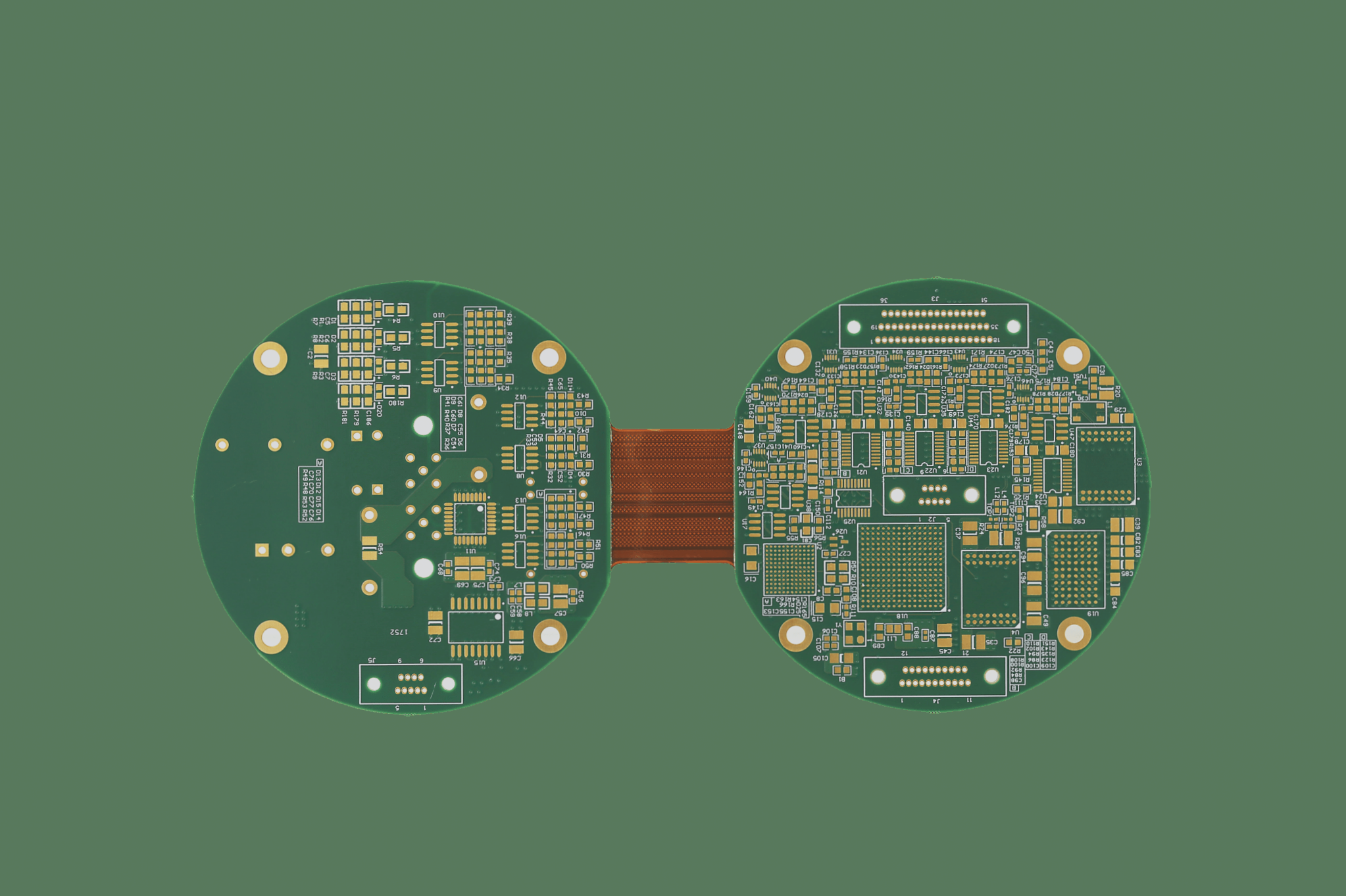
Understanding PCB Circuit Board Features
Through-holes are a common feature in circuit boards, allowing connections between different layers. These holes, visible when held up to light, are created by drilling or laser cutting directly through the board. While some layers may not require these connections, they are crucial for linking specific floors in a multi-layered design, much like connecting floors in a building.
Enhancing PCB Space Utilization
To optimize space utilization in PCB circuit layers, a process called “blind hole” drilling was developed. This method requires precise calibration of drilling depth to ensure accuracy. However, challenges in hole electroplating have limited its adoption among manufacturers.
Advanced Layer Interconnections
For layers that require interconnection, pre-drilled holes can be used before bonding the layers together. This process demands precise positioning and alignment to ensure proper connections.
Complex Layer Connections
Connections between inner circuit layers that do not link to outer layers must be drilled during the creation of individual layers. This labor-intensive process involves partial gluing, electroplating, and bonding all layers together, making it the most expensive manufacturing option.
High-Density Circuit Boards
High-density (HDI) circuit boards utilize intricate layer connections to maximize usable space. This complex production process is reserved for high-density boards, ensuring efficient space utilization across various layers.

 العربية
 简体中文
简体中文 Nederlands
 English
 Français
 Deutsch
 Italiano
 日本語
日本語 한국어
한국어 Português
 Русский
 Español
 ไทย
ไทย