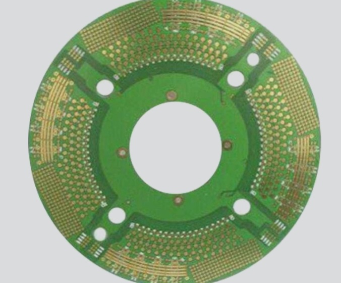
2. The overall trend in electronic technology indicates that products are becoming increasingly complex and compact, leading to a rise in I/Os and circuit board density.
3. Today, it is common for a circuit board to feature more than 20,000 solder joints.
4. Simultaneously, the complexity of the assembly process is escalating.
5. PCB circuit boards typically undergo double-sided SMT assembly, manual assembly, wave soldering, press-fitting, and mechanical assembly processes.
6. Despite manufacturers’ efforts to enhance production capacity and minimize defects, reducing the number of defects on circuit boards remains a challenge.
7. Software tools for testability analysis during circuit board design facilitate collaboration between test engineers and designers, thus helping to decrease time to market.

1. If engineers can anticipate the distribution of faults prior to PCB design layout, develop a testing strategy, and grasp the trade-offs between fault coverage and test access, they will gain a significant competitive edge. This will fundamentally reduce design iterations, simplify challenges, lower production testing costs, enhance manufacturing efficiency, and accelerate time to market.
2. In addition to utilizing software tools that perform testability analysis during circuit board design, manufacturers are exploring alternative testing solutions to minimize development time, expedite new equipment introduction, and ensure high levels of fault coverage and accuracy in the early manufacturing stages.
3. Moreover, the sooner PCB manufacturers can satisfy consumer demand for new products, the greater their potential to capture market share and increase profits. Boosting output in a cost-competitive landscape necessitates effective identification and mitigation of defects at their source, along with understanding root causes and enhancing production capacity.
4. For specific circuit boards, if a distributed test program can effectively balance various factors—such as diagnostic resolution, fault coverage, testability, development time, required skill levels, training costs, working hours, utilization conditions, and overall costs—this approach can yield optimal testing results.
5. How can one develop the ultimate PCB distributed test program? Given that each testing method performs differently across various measurement characteristics, evaluating all combinations is impractical. Addressing this complex issue requires modern software analysis techniques. Without effective quantitative analysis, navigating the multitude of testing options and their intricate, overlapping characteristics will be challenging and time-consuming, likely resulting in suboptimal outcomes.
6. This concludes the introduction to PCB circuit board distributed testing schemes.


