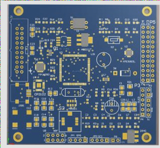
Unlike functional pads that establish electrical connections, non-functional pads are not connected to any traces on the layer they reside. They are typically found on the inner layers of PCBs and do not play a role in electrical functionality.

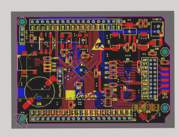
Figure 1: Functional pad vs Non-functional pad
Why retain non-functional pads?
(Preventing over-expansion) When a PCB is heated, the Coefficient of Thermal Expansion (CTE) stresses can lead to warping or delamination. Non-functional pads act as physical barriers, helping prevent excessive expansion of the board.
(Enhancing copper adhesion) Non-functional pads also aid in strengthening copper adhesion on hole walls. Copper plating in vias can be weak along the hole edges. NFPs provide additional metal attachment points, helping prevent plating cracks or delamination.
(Balancing copper weight) Additionally, non-functional pads can be used to balance copper distribution in a PCB. Since copper weight can vary across layers due to high-current copper planes or specific signal paths, NFPs can be strategically placed to ensure even weight distribution, preventing warping or twisting during manufacturing.
Why remove non-functional pads?
(Routing density) Non-functional pads can pose challenges in high-density routing designs. Their presence reduces available space for traces, making it harder to find suitable routing paths, especially when vias are tightly spaced. In such cases, removing NFPs might be necessary to create space for traces. However, this should be done cautiously, particularly for flex and rigid-flex PCBs, as copper plating bonds more weakly to flexible materials. Removing all NFPs can lead to excessive gaps between functional pads, potentially causing plating separation.
(Signal integrity) Another reason to remove non-functional pads is their potential to cause telegraphing. Telegraphing occurs when the copper stack-up of a via becomes visible on the surface of the PCB, typically due to non-functional pads. This can lead to parasitic capacitance and inductance, which may affect signal integrity. If signals travel near such pads, the telegraphed copper may couple with the trace and cause signal reflections, leading to performance issues.
If you have any questions about PCBs and PCBA, please contact us at info@wellcircuits.com


