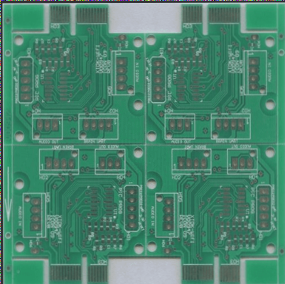
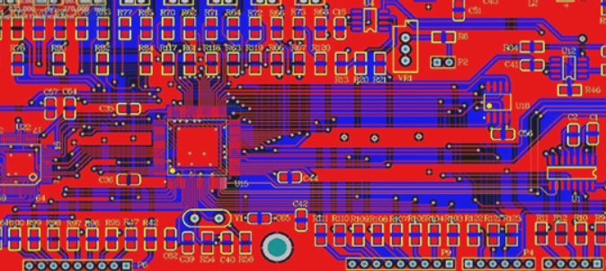
The double sided pcb assembly process is a complicated combination of various steps leading to the final product. These steps should be performed in a strictly defined sequence – otherwise the final product will not meet the initial assumptions. At the PCB design stage, not only the selection of the appropriate technology is important. The precision of assembling the components is also important, as any deviations may determine the correctness of the board.
The Concept Behind Double Sided PCB Assembly Process
A printed circuit board is a very broad concept. It includes both single-layer PCBs made of phenolic-paper laminate, as well as 16-layer (or even more) printed circuit boards manufactured using exotic materials – Teflon, ceramics, etc.
Each of them has a different, often very unique application and each production technology fulfills a certain niche. How do you know about it? You may not have complete knowledge of all PCB technology, but there are some basics you should know.
The article will discuss the subject of the production of printed circuit boards and electronic devices containing such boards, as far as possible. Let’s analyze the whole process from the very beginning, because many aspects influence what and how it is carried out in this process.
PCB assembly technology
Before we delve into the double sided pcb assembly process, let’s discuss some important concepts:
Laminate: the basic material from which the PCB is made. It usually consists of layers of fiberglass bonded with epoxy resin and covered with copper foil on the outer sides.
Copper – a thin layer of this metal, applied on the working layers of the printed circuit, is used to conduct signals.
Soldermask – usually it is a green coating visible on the top of the plate. Its main task is to isolate the copper tracks from the components placed on the board.
Descriptive layer – printing on the solder mask, used to describe the components.
Manual soldering – the process of assembling components on a PCB uses traditional hand tools.
Wave soldering – An industrial soldering process in which printed circuit boards travel through a heated chamber where a molten adhesive is deposited.

Double sided pcb assembly process methods
There are 3 main methods of assembling components on a PCB: through hole assembly, surface assembly and mixed assembly.
Through-Hole Mounting
This type of installation is characterized by the use of components with protruding legs or wires that must be threaded through the holes in the laminate. This method is often found when assembling larger components such as capacitors.
During the assembly of through-hole elements, the following stages can be distinguished:
- The THT components are manually placed on the PCB by the fitter.
- The elements are checked for correct positioning. Any errors are corrected.
All components are mass-soldered in what is known as wave soldering
TH (Through-Hole) components usually have metal leads that must be threaded through holes in the printed circuit board. The resulting connections are characterized by greater mechanical strength than in the case of surface mounting. Due to their simpler structure and larger dimensions, threaded elements are often used in education.
On the other hand, through-hole components require more work – the presence of holes (vias) imposes limitations when designing multilayer boards. Hence, the TH technology is mainly used when assembling larger components and when the system is to be characterized by greater rigidity and mechanical resistance.
Surface Mount (SMT) in double sided pcb assembly process
STM (Surface Mount Technology) is usually used for systems with delicate, miniature components that are difficult to place by hand.
When assembling surface elements (SMD), the following stages can be distinguished:
A special template for solder paste is designed in double sided pcb assembly process. It will be used to apply the binder in the form of a paste, only in the places where the terminals of the components will be.
The components are placed on the board at the pick and place stage of machine assembly.
The board with components is heated in a soldering oven to melt the solder paste and bond the components to the copper tracks.
An interesting solution in the industrial assembly of surface elements is the use of solder paste. It consists of a mixture of fine grains of the binder and the flux. The solder paste is not only used for soldering, it also provides the necessary adhesion so that the components do not slide over the laminate surface.
A special template is used to make the application of the solder paste easier and more precise. It is attached to the PCB and then the solder paste is pressed into the holes in the template with the help of a roller.
Mixed mounting in double sided pcb assembly process
This type of assembly is the result of limitations in the miniaturization of components and different requirements for their strength. It combines surface and through-hole technology so that it is possible to assemble various types of components.
This assembly is more complicated, hence the following cases can be distinguished:
- on one side of the board there are both SMT and THT components,
- SMT components are placed on one side of the board, and THT on the other side,
- On both sides of the board there is a mixture of SMT and THT components.
Regardless of the arrangement of components, mixed assembly makes it difficult to automate the placement of components. Pick and place machines must be enriched with a more complicated set of procedures so as to deal with different sizes of elements so as not to collide with them.
Also, the soldering of a board prepared in this way poses some difficulties. In the case of a board coated on both sides, soldering is required on both sides of the board. However, it is impossible to use the popular wave method, as some of the components would be damaged.
Elements of double sided pcb assembly process
After the printed circuit board is made, it is necessary to install and solder the electronic components on its surface. Depending on the mounting method, electronic components can be through-hole (THT) and surface mounted. Therefore, the approach to their assembly and soldering is different.
Of course, all tiles can be installed by hand, but in many cases this is not the best solution. Simple prototypes can be assembled in this way, while in the case of mass production, or even more complex prototypes (e.g. with systems in BGA casings), automatic assembly is much more reasonable.
Placing components on the PCB using the pick and place machine
The first step of assembly is to put solder paste and glue on the PCB, if required by the SMD components used (e.g. when they are heavy or are on both sides of the PCB). The elements are then applied to the solder paste applied to the solder pads.
In most cases, the so-called pick and place machines that take elements from tapes or trays and place them automatically in their place on the surface of the printed circuit board.
The information required for this is saved in a special Pick & Place file, which we wrote about earlier. In this way, SMD and THT elements are assembled (the latter not always – not all through-hole elements are compatible with automatic assembly).
Process of Applying paste in double sided pcb assembly
The PCBs with the paste applied and the components installed must then be soldered. This is done in two ways, depending on the type of components – SMD and THT.
The first ones are soldered in the so-called reflow. The plates are passed through a tunnel oven in which they are gradually heated up to the solder paste melting point, which permanently binds the elements together.
The tiles are then cooled in a controlled manner to prevent them, for example, from warping. The through-hole elements are soldered using the so-called wave – a stream of dissolved solder, washing the bottom side of the PCB and flooding the protruding terminals of the elements.
Summary: double sided pcb assembly process
The above article outlines the topics related to double sided pcb assembly process. Of course, the above description cannot be considered exhaustive in any way. On the one hand, only the most popular, according to the author, PCB production technologies are shown, and on the other hand, many important details concerning the production of printed circuits are not discussed.
Aspects such as metallization, necessary for the production of vias and the application of galvanic layers (mainly gold), application of an anti-solder layer (soldermask) or description, as well as drilling and milling of PCBs, were omitted. However, this article should be a good starting point to explore the nuances of PCB manufacturing technology.


