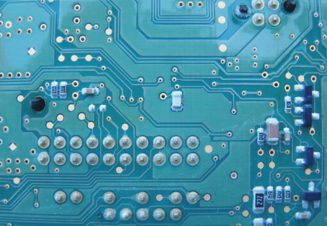
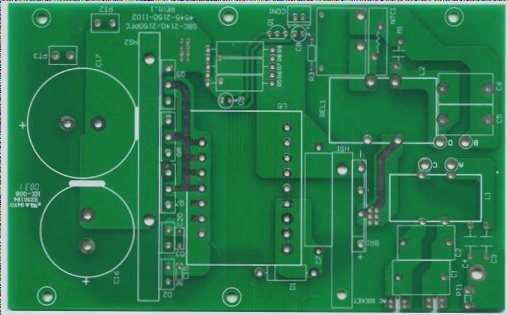
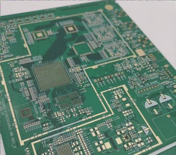
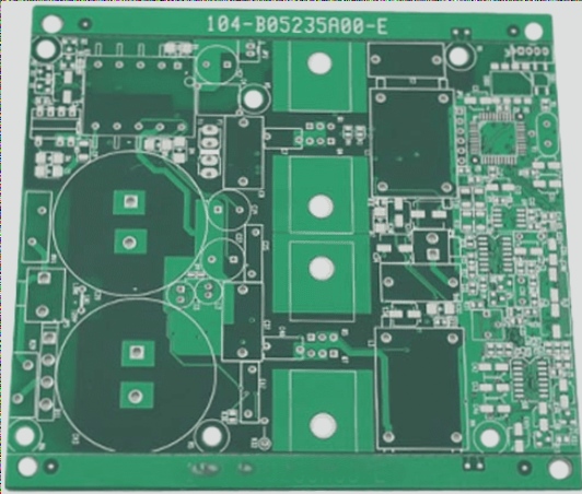
In order to establish electrical connections between the layers of the circuit, the boards must undergo a drilling process to create holes according to the specifications outlined in the drill files. For single- and double-sided boards, drilling typically follows board cutting. However, for multi-layered boards, drilling occurs after lamination. The PCB drilling process can generally be divided into the following four key steps:
1. Drilling Location Holes
Location holes act as reference points for PCB production and testing. Before drilling, the backup board, the substrate, and the aluminum sheet are arranged on the high-speed drilling machine’s table, starting from the bottom and working upwards. According to the manufacturing instructions, three to four location holes, each around 3.2 mm in diameter, are drilled along the edges of the board.
2. Inserting Pins
To improve production efficiency, multiple boards are stacked together for the drilling process. These boards are first secured to the drilling machine’s table using pins that hold the backing board and the cover plate in place, preventing any shifting or misalignment during drilling.
3. Drilling Holes
The drilling process is controlled by a computer program, which reads the CAM-converted drilling parameter files to create the required holes. Mechanical drilling is a widely used technique for creating holes in PCB manufacturing. The drill bit, powered by the spindle, rotates at high speed to apply cutting force, drilling various types of holes, such as Plated Through Holes (PTH), Non-Plated Through Holes (NPTH), and Via Holes. To protect the drilling machine surface, a backup board is placed underneath the PCB, and an aluminum sheet is laid on top to ensure flatter holes in the copper foil and prevent overheating of the drill bit.
If you have any questions about PCB or PCBA, please feel free to contact me at info@wellcircuits.com.


