**PCB Component Dynamic Analysis and PCB Proofing**
For avionics, failures due to vibration and shock can significantly reduce reliability and lead to extremely severe consequences. PCBs are often subjected to real-time vibration testing in avionics systems. By conducting dynamic analysis and optimizing the design of PCB components, the likelihood of failure during environmental testing can be effectively minimized, thus enhancing the reliability and quality of avionics.
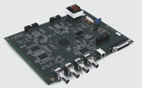
Dynamic analysis is based on the assessment of dynamic characteristics. A dynamic model of the PCB assembly can be developed through this analysis. Only by creating an accurate kinetic model can effective dynamic analysis be performed. In this regard, this paper aims to apply pre-test techniques such as Finite Element Analysis (FEA) and Experimental Modal Analysis (EMA) to investigate the dynamic properties of avionics PCB components (as illustrated in Figure 1), and to develop a limited Metadynamic analysis model for the PCB components.

1. **Limited Deterioration Analysis**
Finite element analysis (FEA), as a mature numerical analysis technique, is widely used to statistically analyze the dynamic characteristics of PCB components in electronic devices. Furthermore, FEA assists engineers in designing more reliable PCB assemblies by predicting potential failures and fatigue early in the design phase. This article focuses on the PCB assembly used in avionics (Figure 1) as the research subject. The dimensions of the PCB are 133.5mm in length, 79mm in width, and 1.8mm in thickness, with the assembly fixed at the four corners of the PCB onto the housing of the electronic device using screws. The external dimensions and mounting method of the PCB components closely align with the standard test PCBs in terms of size and fixation, though the thickness is slightly greater. Components and connectors are assembled onto the PCB via surface mount technology (SMT), with the primary packaging types being BGA, QFP, and SOP.
2. **Finite Element Analysis Model**
The material properties for each part of the PCB assembly are considered when developing the finite element analysis model. Using the geometric and material data of the PCB components, a finite element model was constructed in ANSYS. Since the goal is to obtain the dynamic performance of the entire PCB assembly rather than the detailed behavior of individual components, simplifications were made during model construction. Specifically, rectangular and square blocks were used to represent components, while their approximate shapes were used for the connectors. Each part of the finite element model was meshed using three-dimensional solid elements (SOLID187). While this approach increases the computational effort, it significantly reduces the workload from CAD to CAE, facilitating broader engineering application. Multi-point constraints (MPC) were applied to model the connections between the components and the PCB. Additionally, because the rigidity of the electronic housing is much higher than that of the PCB assembly, fixed support constraints were applied to the screw holes at the four corners in the finite element model to simulate the attachment of the PCB to the device housing.
3. **Finite Element Analysis Results**
A finite element model of the target PCB assembly was created, and the Block Lanczos method was employed for modal analysis. Modal analysis involves solving the system’s characteristic equation, which, for a general multi-degree-of-freedom system, provides the system’s characteristic values and vectors—namely, the natural frequencies and vibration modes of the PCB system.
In the finite element modal analysis, the mass matrix of the PCB system was assembled from the element mass matrices, and the stiffness matrix was constructed from the element stiffness matrices.
The modal analysis results revealed the first and third natural frequencies and vibration modes of the PCB assembly secured by four screws. The first-order mode of the PCB assembly corresponds to bending, while the second-order mode is also a form of bending. The third-order mode is torsional, and the fourth-order mode is characterized by sinusoidal wave bending. These vibration modes closely resemble those observed in a PCB secured with four screws, such as those in a JEDEC standard test board.
If your have any questions about PCB ,please contact me info@wellcircuits.com


