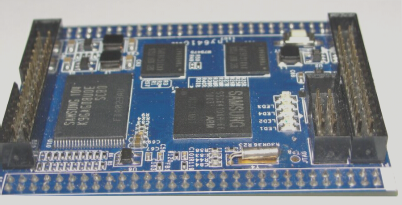
PCB Design Challenges and Solutions
PCB design is a meticulous process that demands attention to detail to ensure accuracy. Engineers face challenges such as manual checks and potential errors, making the process labor-intensive.
Key Steps in PCB Design
- Schematic capture
- Schematic verification
- Layout design
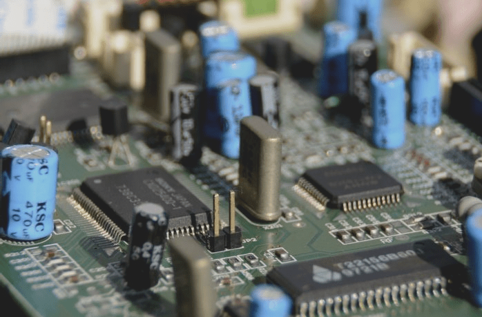
During schematic capture, engineers may encounter common issues like underscore errors, case sensitivity problems, and spelling mistakes. These errors can lead to design flaws and signal short circuits.
Importance of Schematic Simulation
Schematic simulation is a crucial tool in PCB design that automatically checks for errors, reducing manual inspection time. It helps verify connections and ensures the design meets functional expectations.
By utilizing schematic simulation, designers can identify errors quickly, leading to faster design processes and fewer revisions.
Enhancing Efficiency in PCB Design
Advanced design tools and best practices, such as design rule checks and electrical rule checks, can improve efficiency and accuracy in PCB design. Automated tools for tasks like signal integrity analysis and thermal management enhance design reliability.
Conclusion
PCB design requires precision and efficiency. Leveraging tools like schematic simulation and design verification techniques can minimize errors and improve overall design quality, saving time and ensuring functional products.
Efficient Design Verification with Schematic Simulation
In complex PCB designs, efficient tools like schematic simulation are essential to accelerate the design process and enhance circuit quality. By verifying connections and ensuring proper functioning, engineers can improve process efficiency.
Device Under Test (DUT) in PCB design involves various signals and modules, such as voltage regulators and operational amplifiers. Schematic simulation aids in verifying circuit connections through creating a schematic, developing a test platform, and running simulations for comprehensive design verification.
The Importance of Schematic Simulation in PCB Design
Connecting a probe to the nodes of interest streamlines the design process. Monitoring voltage and waveforms helps identify errors in the schematic quickly. The simulation automatically checks signal connections to ensure all components function as expected.
Benefits for PCB Manufacturers
- Schematic simulation reduces design errors and improves efficiency.
- Real-time monitoring of nodes and voltages provides a clear view of circuit behavior.
- Designers can directly observe simulation results to confirm schematic correctness.
Exploring Design Adjustments
Schematic simulation allows designers to easily explore design adjustments. By modifying stimulus signals or component values, the impact of changes can be simulated before implementation on the physical PCB. This flexibility reduces design errors and enhances product accuracy.
Time-Saving and Quality-Enhancing
Schematic simulation saves time for circuit board designers and inspection teams. It increases the probability of achieving a correct design by allowing detailed verification and adjustments, thus enhancing the speed and quality of the PCB design process.