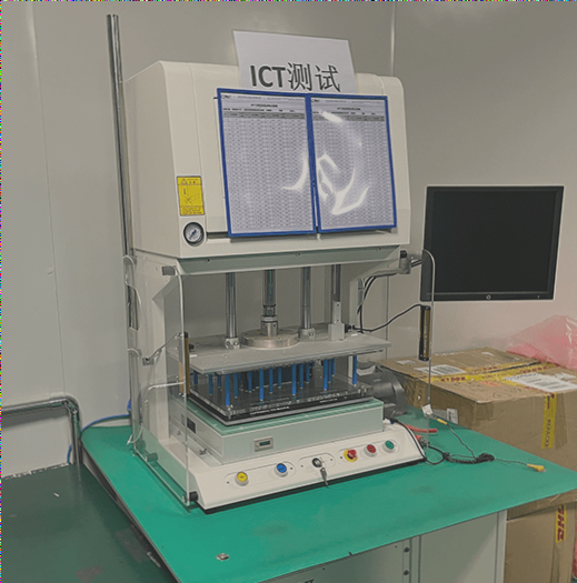
Flying Probe Testing in PCB Manufacturing: An Effective Approach
The flying probe test is a commonly used method in PCB manufacturing to verify the electrical functionality of printed circuit boards, especially for identifying open circuits and shorts. This testing technique involves a test probe connected to a driver and a sensor through a multiplexing system, allowing for the testing of individual components on the Unit Under Test (UUT). While one component is tested, the prober shields the remaining components electrically to prevent interference in readings.
Key Steps in Developing a Flying Probe Test Program:
Method 1: Program Creation Process
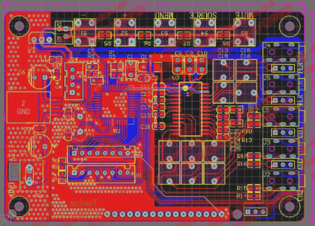
- Importing the PCB Layer Files: The initial step involves importing the PCB design files, typically in formats like Gerber or ODB++, containing information about the PCB’s different layers.
- Layer Review and Organization: After file import, reviewing and organizing the layers is crucial to ensure accuracy and completeness, with each layer named according to its function.
- Layer Renaming: Renaming the outer layers as “front” and “rear” and internal layers for clarity and efficient test programming.
- Alignment and Calibration: Aligning and calibrating the layers and probes to match the PCB’s physical layout for accurate testing.
- Test Point Selection: Verifying critical test points like vias, pads, and components for testing.
- Test Program Optimization: Optimizing the test program to enhance accuracy and minimize testing time by adjusting probe movement paths and prioritizing test points.
Advantages of Flying Probe Testing:
- Flexibility: Adaptable to various PCB designs without custom fixtures.
- Reduced Setup Costs: Lower setup costs as custom test fixtures are not required.
- Fast Turnaround: Ideal for prototype and low-volume production due to faster testing.
- Precision: Allows precise testing of components across the PCB.
Developing a reliable flying probe test program ensures efficient and accurate electrical testing of PCBs in a manufacturing setting.
Step-by-Step Process for PCB Testing with Ediapv Software
Second Step: Layer Management
To manage layers effectively, add new layers to the PCB design by copying existing solder mask and drilling layers. Rename these new layers for front and rear negative test points and hole definitions. For designs with blind and buried vias, assign sequential names to represent different via configurations.
Adjusting Test Point Sizes
Modify the duplicated fronmneg and rearmneg layers to use round test points with an 8 mil D code. Label fronmneg as the “front test point” and rearmneg as the “rear test point.” This adjustment ensures that test points are appropriately sized for flying probe testing.
Hole and Via Management
- Delete the NPTH (Non-Plated Through Hole) from the design.
- Identify the via holes based on their connections in the layout, and designate any untested holes accordingly.
This step ensures that the layout is properly prepared for testing by removing unnecessary elements and defining holes that require testing.
Reference Layer Setup and Test Point Alignment
- Use the fron and mehole layers as reference layers.
- Change the fronmneg layer to the “on” state and verify that all test points align within the window of the front layer.
Test points associated with holes larger than 100 mil should be moved to the soldering ring area for easier access during testing. In cases where BGA test points are too dense, misalignment may be required to optimize space. Additionally, redundant intermediate test points can be removed to reduce clutter.
Copy Test Points to Front and Rear Layers
- Copy the organized test points from fronmneg to the fron layer.
- Copy the test points from rearmneg to the rear layer.
This step ensures that test points are accurately placed on the corresponding layers for both sides of the PCB.
Layer Activation and Positioning
Activate all layers in the design and move the layout to the origin point (10,10mm) for consistency and easier reference.
Naming and Output Gerber Files
Output the Gerber files with the following layer names:
- fron
- ily02, ily03, ily04neg, ily05neg
- rear
- fronmneg, rearmneg, mehole
- met01-02, met02-09, met09-met10
These Gerber files represent all the necessary layers for the PCB manufacturing and testing process.
Using Ediapv Software for Test Generation
Step 1: Import Gerber Files
Import all the Gerber files (e.g., fron, ily02, ily03, ily04neg, ily05neg, rear, fronmneg, rearmneg, mehole, met01-02, met02-09, met09-met10) into Ediapv.
Step 2: Generate Netlist
Click the “Generate Network” option and use the “Net Annotation of Artwork” button to assign net labels to the layers.
Step 3: Create Test Files
Select the “Make Test Programs” button in Ediapv. When prompted, enter the D code for the untested holes. This will generate the necessary test program files for the flying probe machine.
Step 4: Save the Test Files
Save the generated test files to a specified location for later use.
Step 5: Set Reference Point
Finally, set the reference point for the PCB layout and complete the preparation. The test program is now ready to be transferred to the flying probe machine for testing.
Key Points and Considerations
- Intermediate Test Points: Review and remove redundant test points manually to avoid unnecessary clutter.
- Handling MEHOLE Windows: Ensure proper test program generation for MEHOLE windows on both sides of the PCB.
- Connectivity Test Challenges: Validate generated connectivity tests to ensure accuracy, especially for holes without corresponding lines.
- Rear Layer Solder Mask: Rename the REAR layer to prevent irrelevant test point generation in the absence of window openings.
By following these steps and tips, PCB designers and manufacturers can ensure a smoother and more accurate process for generating test files and conducting flying probe tests.