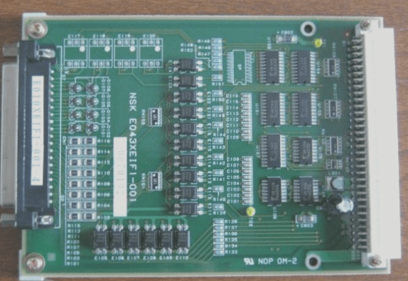
Determining PCB Layer Count
When designing a PCB, it is crucial to determine the number of routing layers early on. Factors such as board size and the presence of high-density components like Ball Grid Array (BGA) components impact the required number of layers. The stack-up method and board size directly influence routing and impedance characteristics. While fewer layers were once believed to reduce costs, recent trends show that the cost gap between different layer counts has narrowed. Using more layers and distributing copper evenly from the start can help avoid signal integrity issues and the need for additional layers later in the design process.
Design Rules and Signal Constraints
For successful routing, it is essential to establish clear design rules and constraints. Different signal lines have specific routing requirements, and each signal class should be assigned a priority level based on these requirements. Factors such as trace width, via count, parallelism, and layer limitations significantly impact routing tool performance. Adhering to these rules ensures efficient and accurate routing.
Optimizing Component Layout
Designing for manufacturability (DFM) rules dictate component layout restrictions to streamline the assembly process. Careful consideration of routing channels and via areas is necessary to facilitate automated routing. By setting appropriate constraints and layer definitions, designers can guide the routing tool to achieve the desired layout.
Effective Fan-Out Design
During fan-out design, each pin of a surface-mount device (SMD) should have at least one via for inner layer connectivity and testing purposes. Using larger vias and wider traces with a suitable via interval enhances the efficiency of the routing tool. Considering in-circuit testing early on and selecting the right via type are crucial for cost-effective production.
Manual Routing for Critical Signals
While automated routing is essential, manual routing plays a significant role in PCB design, especially for critical signals. Manual routing, either standalone or in combination with automated tools, ensures that performance requirements are met. Verification by engineering personnel is key to finalizing the design.
Utilizing Automatic Routing
Key Considerations for Routing Critical Signals
When routing critical signals on a PCB, it is crucial to focus on minimizing distributed inductance and addressing electromagnetic compatibility (EMC) issues. Utilizing EDA tools can assist in controlling these parameters effectively, ultimately improving the automated routing outcome.
Guidelines for Automated Routing
Establishing specific constraints and defining routing areas are essential for automated routing success. By setting limitations on layer count and via usage, engineers can guide the routing tool to align with their design philosophy, preventing unnecessary vias and optimizing signal paths.
Optimizing Automated Routing
Automated routing tools can generate results close to expectations once constraints are in place. However, manual intervention may still be necessary to fine-tune signal routing and network connections. Locking completed designs can safeguard against unintended alterations during subsequent routing processes.
Efficient Design Tips for Automatic Routing
- 1) Experiment with different routing paths by making slight adjustments to settings.
- 2) Maintain consistency in basic rules while exploring various routing parameters like layers, trace widths, and via types to observe their impact on the design.
- 3) Allow the routing tool to manage default networks efficiently.
- 4) Adjust the level of automation based on signal criticality to optimize routing outcomes.
Finalizing the Routing Process
Reviewing routing length data can help identify excessively long signal routes or areas with limited constraints. Manual editing may be required to shorten traces and minimize vias, ensuring optimal signal integrity. During finalization, evaluate and refine routes to enhance overall design quality.
Balancing PCB Aesthetics with Functionality
While aesthetics were once a priority in PCB design, modern automated approaches prioritize electrical performance. While automatically routed PCBs may lack visual appeal compared to manual designs, they excel in meeting electrical requirements and performance standards.
For inquiries regarding PCB or PCBA services, please reach out to us at info@wellcircuits.com.