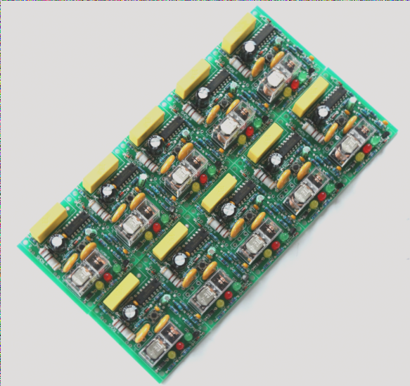
PCB Production Challenges and Solutions
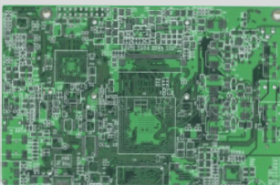
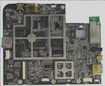
Automotive PCB production faces inevitable electrical defects like short circuits, open circuits, and leakage due to external factors. As PCBs become more complex with higher density and finer pitch designs, the risk of defects increases. Detecting and addressing these issues early is crucial to reduce waste and costs.
Cost of Defects in PCB Manufacturing
Defect-related costs vary at different production stages. The “Rule of 10’s” demonstrates how costs escalate as defects progress. Early detection is key to minimizing remediation expenses. For instance, fixing an open circuit on a blank board is far cheaper than addressing the same issue during later assembly stages.
Importance of Electrical Testing
Effective electrical testing is vital for detecting functional circuit defects early in the PCB production process. Failure to identify defects can lead to significant losses in end products like computers and mobile phones. Testing technology optimization and process control are essential to reduce defect-related costs and improve overall yield.
PCB Electrical Testing: Best Practices
PCB manufacturers often conduct 100% electrical testing as per customer requirements. Key elements like test data source, conditions, equipment selection, and repair specifications are defined beforehand to ensure consistency and accuracy.
Stages of Electrical Testing
- Post-Inner Layer Etching
- Post-Outer Layer Etching
- Finished Product Testing
Each stage involves multiple rounds of testing to identify and rework defective boards. Test stations aid in data collection for defect analysis, enabling manufacturers to take targeted corrective actions.
Electrical Testing Methods
Common testing methods include dedicated testing, universal grid testing, and flying probe testing. These methods help in identifying defects like open circuits, short circuits, and insulation failures, allowing for improved quality control.
Comparison of Testing Methods:
- Dedicated Test Equipment
- Universal Grid Test Equipment
- Flying Probe Test Equipment
Dedicated Testing
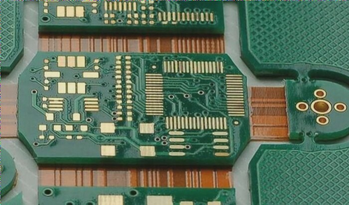
Dedicated testing utilizes specialized fixtures like needle plates tailored for specific PCB material types. These fixtures are not interchangeable between different material types, limiting their adaptability. Dedicated testers can examine up to 10,240 points for single-sided boards and 8,192 points for double-sided boards. This method is commonly used for boards with larger pitch sizes due to the probe size precision. While highly accurate for specific boards, it is not suitable for high-mix or small-batch production.
Universal Grid Test Equipment
Universal grid testing follows a fixed grid layout where the PCB circuit is designed with specific hole positions. A G10 base material acts as a mask, with electrical probes testing only the designated hole positions. This method is cost-effective, quick to set up, and the probes can be reused across different designs. Universal grid testers often feature automated systems capable of conducting **open/short** electrical tests, usually at **high voltage levels** (e.g., 250V). A typical universal grid tester has **10,000+ test points**, making it suitable for mid- to high-volume production. However, for high-density boards with very tight spacing (such as QFP packages), an off-grid fixture design may be necessary, and the test density is limited by the design of the grid and the spacing between components.
Flying Probe Test Equipment
The flying probe test method involves moving two probes in the X, Y, and Z directions to test the endpoints of each circuit. Unlike other methods, flying probe testing does not require dedicated fixtures, making it ideal for smaller runs or prototypes. However, the trade-off is slower test speeds—typically around **10-40 points per second**. Flying probe testing is well-suited for high-density boards, as it can accurately test circuits with tight spacing. Despite its slower testing speed, it is an excellent option for low-volume or prototype production where flexibility is paramount.
Comparison Summary
- Dedicated Test: Fast, Low Flexibility, Moderate Test Density, Custom, not reusable fixtures, Ideal for High-volume, single material designs
- Universal Grid Test: Moderate Test Speed, Moderate Flexibility, High Test Density, Reusable, fixed grid fixtures, Ideal for Medium-to-high volume, high-mix production
- Flying Probe Test: Slow Test Speed, High Flexibility, Very High Test Density, No fixture needed, Ideal for Low-volume, prototype, high-density boards
Conclusion
The choice of the right electrical testing method depends on various factors, including production volume, PCB design complexity, and test density requirements. Dedicated test equipment suits high-volume production with low material variation. Universal grid test equipment provides a good balance of speed and flexibility for medium-to-high volume production. Flying probe testing, though slower, offers high flexibility and is ideal for prototypes and low-volume runs with complex or high-density designs. Each method has its unique advantages, and understanding these trade-offs helps manufacturers select the most efficient testing solution for their specific needs.