Enhancing Electromagnetic Compatibility in PCB Design
Introduction
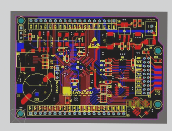
Electromagnetic compatibility (EMC) design is crucial in the circuit board design process to prevent reliability and stability issues in electronic products. Common problems such as signal distortion, excessive noise, and system crashes can be avoided with proper EMC design. This article provides practical insights on enhancing EMC from layer design to layout.
Layer Configuration

- The layers of a PCB consist of power, ground, and signal layers. Proper organization and classification of these layers are essential for effective design. Allocating different power supplies to separate layers and adding ground planes for special signals can enhance EMC.
- Designing the power layer involves considering the type and number of power supplies. Multiple power layers may be needed for high-power applications or circuits with multiple power sources to avoid overlap between power domains.
- Signal layer design should prioritize special signal routing and shielding. Using dedicated ground plane layers for sensitive signals can improve EMC. Avoid designing single-sided or double-sided PCBs for complex circuits due to limited signal density and shielding.
PCB Layer Layout Design
- Position the power plane next to the ground plane to create a coupling capacitor for impedance reduction and filtering.
- Choosing the ground plane as the reference plane is preferred for better shielding and EMC.
- Avoid crossing key signals between adjacent layers to reduce radiation and coupling.
- Avoid routing signal traces on the ground plane to maintain its integrity. Consider routing on the edge of the power plane for high signal trace density.
PCB Layout Best Practices for Signal Integrity
- Design a solid ground plane under critical signals to reduce radiation.
- Consider power supply radiation and interference by ensuring the ground plane shields the power supply effectively.
General Principles for Multi-Layer PCB Layout:
- Place the power plane near or below the ground plane.
- Keep signal layers adjacent to the entire metal plane.
- Isolate digital and analog signals to prevent mixing.
- Use physical separation like slots to isolate different signal types.
- Inner layer traces act as planar waveguides, while outer layer traces form microstrip lines.
- Keep clock and high-frequency circuits away from sensitive areas to reduce interference.
- Treat stray currents and high-frequency radiation currents differently across layers.
Layer Design and Layout for Enhanced EMC:
The number of layers depends on power, ground, high-frequency, special, and sensitive signals. Focus on minimizing coupling, optimizing routing, and carefully placing different signal areas for improved electromagnetic compatibility.