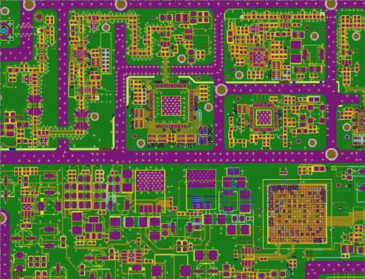
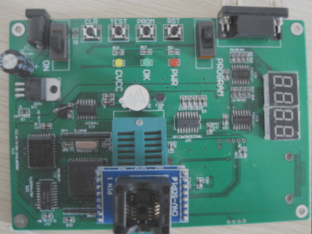
1. For the noise on the PCB board, when electromagnetic interference is detected in the digital circuit, the primary indicator is the presence of noticeable noise voltage on the power line and ground line, observable with an oscilloscope.
2. While many can identify these noises as the source of electromagnetic interference issues in circuits, they often lack solutions for addressing them.
3. To effectively eliminate noise, it is crucial to first understand how these noises are generated.

1. **Noise on the Power Line**
For a typical gate circuit output stage, when the output is high, Q3 is turned on and Q4 is turned off; when the output is low, Q3 is turned off and Q4 is turned on. In both states, a high impedance is created between the power supply and ground, which limits current flow from the power supply. When the state changes, Q3 and Q4 are momentarily turned on simultaneously. This creates a temporary low impedance between the power supply and ground, resulting in a peak current of 30-100 mA. As the gate output level changes from low to high, the power supply must not only maintain the output current but also charge the parasitic capacitance to handle this current peak. Due to the inductance in the power line, a sudden change in current generates an induced voltage, which manifests as noise on the power line. This noise is accompanied by a brief voltage dip caused by the power line’s impedance.
2. **Noise on the Ground**
When the aforementioned peak current occurs, it also flows through the ground wire. Especially when the output level changes from high to low and the parasitic capacitance discharges, the peak current on the ground wire is higher. Since the ground wire also has varying degrees of inductance, an induced voltage generates ground wire noise. Both ground and power line noise can adversely affect circuit performance and produce significant electromagnetic radiation.
“Icc” (current on power supply): The amplitude varies with different output states. When stable, the current remains constant. During a low-to-high output transition, there is a brief short circuit, causing an increase in current as the parasitic capacitance charges; during a high-to-low transition, there is also a brief short circuit, but since the parasitic capacitance is discharged simultaneously, the current peak is lower than during a low-to-high transition.
“Vcc” (voltage on power supply): Abrupt changes in Icc lead to an induced voltage of “Ldi/dt” due to the inductance L of the power line.
“Ig” (ground current): This refers to the current on the power line and the discharge of parasitic capacitances. With stable output, the current remains steady. During a low-to-high transition, there is an instantaneous short circuit and current increase; during a high-to-low transition, there is also an instantaneous short circuit and current increase, with simultaneous discharge of parasitic capacitance, resulting in a higher current peak compared to the low-to-high transition.
“Vg” (ground wire voltage): Abrupt changes in “Ig” induce a voltage “Ldi/dt” in the ground wire due to its inductance L.
**Power Line and Ground Line Noise Voltage Waveform**
To address noise voltage on the ground line, placing a grid on the circuit board can reduce inductance, though it occupies significant wiring space. To minimize power supply line inductance, consider using energy storage capacitors, which provide the large currents needed during circuit output state changes, thus reducing induced noise voltage and avoiding current spikes. Storage capacitors limit current variations and reduce radiation, so it’s beneficial to add these capacitors alongside power line grids or power planes on the circuit board. To provide transient high energy to the chip, place the energy storage capacitor as close to the chip as possible, minimizing the area of the power supply circuit and the distance between the capacitor and the chip’s power and ground terminals. Keep traces as short as possible. The length of the trace between the chip and the energy storage capacitor should be limited to the length of the chip’s pins plus the length of the circuit board trace. Therefore, select chips with closely spaced power and ground pins, and avoid using surface-mounted chips or chip mounts. Additionally, after each discharge of the energy storage capacitor, timely recharge it to prepare for the next discharge. To minimize disturbances to the power supply system, use a secondary energy storage capacitor. For a circuit board with a few chips, place a secondary energy storage capacitor at the power line entrance, with its capacity at least five times that of the chip energy storage capacitors. For boards with many chips, add a secondary energy storage capacitor every 5 to 10 chips. Use tantalum capacitors for this purpose, ensuring minimal series inductance, and avoid aluminum electrolytic capacitors to prevent internal inductance on the PCB.


