Printed Circuit Boards (PCBs): The Backbone of Electronic Connections
The Evolution and Advantages of PCBs
- PCBs have been in development for over a century, focusing on efficient layout planning.
- They offer a significant reduction in wiring and assembly errors, enhancing automation and production efficiency.
- PCBs come in various layers, from single-layer to multi-layer designs, improving precision and reliability.
- China leads the global PCB manufacturing industry with rapid growth and cost efficiencies.
The Future of PCB Technology
The future of PCB manufacturing technology is moving towards high density, precision, and reliability, ensuring their vitality in electronic product development. Key trends include:
- High-speed transmission
- Lightweight and thin designs
- Multi-layer configurations
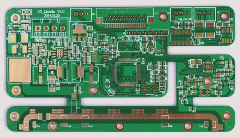
Components of a PCB Circuit Board
A PCB circuit board consists of:
- Circuits and Drawings: Conduct electricity between components with a large copper surface for grounding and power.
- Dielectric Layer: Insulates circuits and layers, also known as the substrate.
- Through Holes: Connect circuits and allow for component plug-ins.
- Solder Mask: Prevents tin spread and short circuits, available in various colors.
- Silkscreen Layer: Marks component names and positions for easy maintenance and identification.
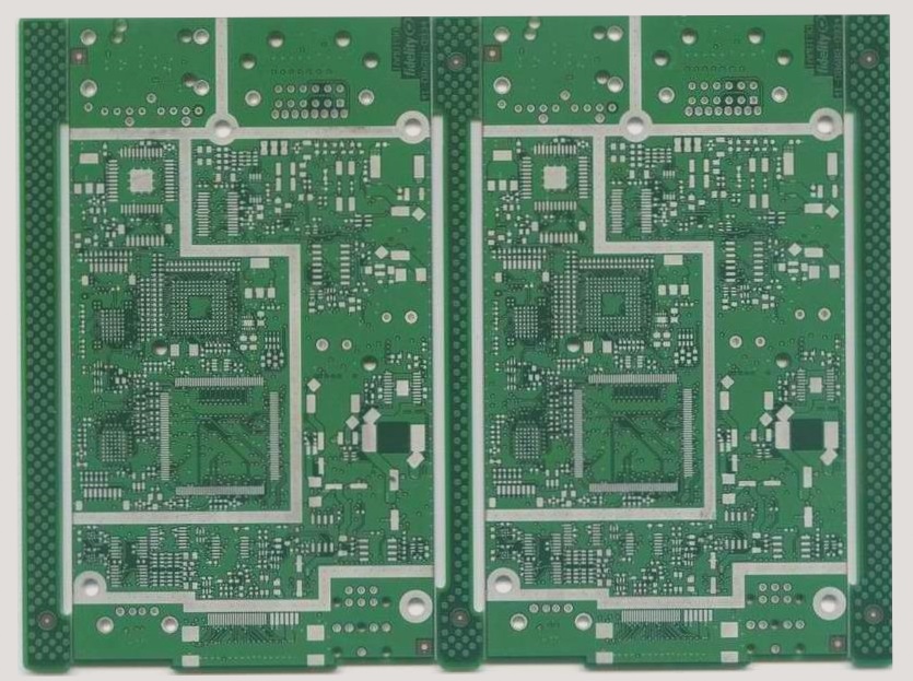
Optimizing PCB Layout for Performance
Efficient PCB layout is crucial for performance:
- Uniformly place components for easy processing, inspection, and maintenance.
- Minimize lead lengths and connections for a consistent packing density.
- Avoid intersecting high and low-level signals and keep transmission lines short.
With continuous advancements in technology, PCBs remain essential for the seamless functioning of modern electronic devices.