Introduction:
Miniaturization and multifunctionality are the primary drivers behind the growth of the electronics industry. The printed circuit board (PCB) serves as the most common platform for electronic assemblies. This includes rigid or flexible polymer substrates, as well as ceramic substrates for metal wiring. Typically, various components and subsystems are mounted on the PCB’s surface. However, to reduce the number of surface-mounted components, researchers are constantly exploring ways to optimize the spatial layout of the PCB and embed components within the board.
Advantages of Embedding Components into PCBs:
- Shorter trace lengths and simplified layout.
- Improved system reliability due to fewer soldering points.
- More stable electrical properties, especially at high frequencies, due to reduced parasitic effects.
- Lower costs as embedded components are cheaper than surface-mounted components.
Currently, various technologies for embedding components into PCBs are rapidly advancing, though no single technology has claimed an absolute lead.
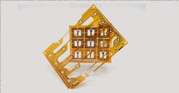
Embedding Passive Components into Flex-PCBs:
Embedded passive components primarily include capacitors and resistors. Numerous methods have been developed to embed these components:
- Capacitors can be embedded by etching the upper and lower electrodes on a dielectric diaphragm with copper cladding on both sides, followed by layering to form the embedded capacitors. Alternatively, paste or sputtered films can be used to form the dielectric and electrode layers.
- For resistors, polymer resistor paste can be printed onto copper foil electrodes. Electroplating of the resistor film between the copper foil and the substrate is another method, followed by etching to create the lines and resistive elements. Additionally, ceramic thick film slurry can be printed, and high-temperature sintering can form capacitors and resistors before lamination to embed the components.
These techniques are commonly applied to rigid PCBs. However, for flexible PCBs, special considerations are required due to the bending nature of embedded components. The following section introduces a novel method for embedding film resistors into flexible PCBs.
Embedding Resistors Using Electroless Nickel Plating:
Electroless nickel plating of films with a thickness of less than 100nm is a commercially feasible method for forming resistive elements on printed circuit boards.
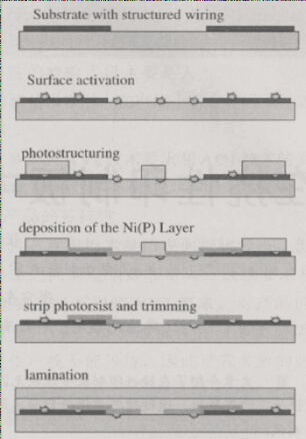

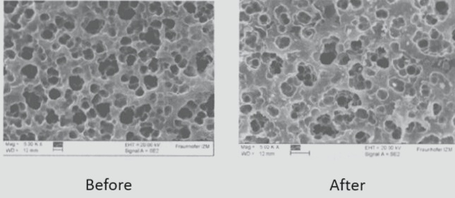
This process allows the production of resistors with resistance values between 25Ω and 50Ω. Due to the flexible substrate’s manufacturing process, the underlying PI (polyimide) shows a spongy surface after the copper is etched away. As the nickel film is less than 100nm thick, the surface morphology remains relatively uniform, except in areas where nickel overgrowth forms clusters.
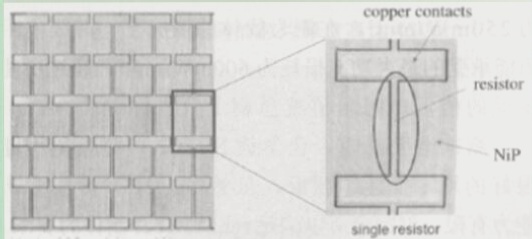
Film Resistor Performance Testing:
To facilitate testing, a specialized circuit diagram was designed, with each board containing 400 test resistors. The process was modified by depositing a nickel film over the entire surface of the board and then using a laser to cut the resistance pattern.
Conclusion:
The results demonstrate that the electroless nickel plating process can be applied to flexible circuit boards. While the bending capacity of the nickel film is limited, it sufficiently meets the requirements for the reel-to-reel process.
Contact Information:
If you have any questions about PCBs or PCBA, feel free to contact us at info@wellcircuits.com.