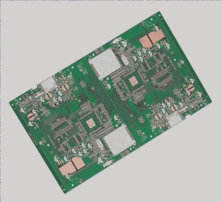
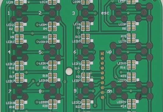
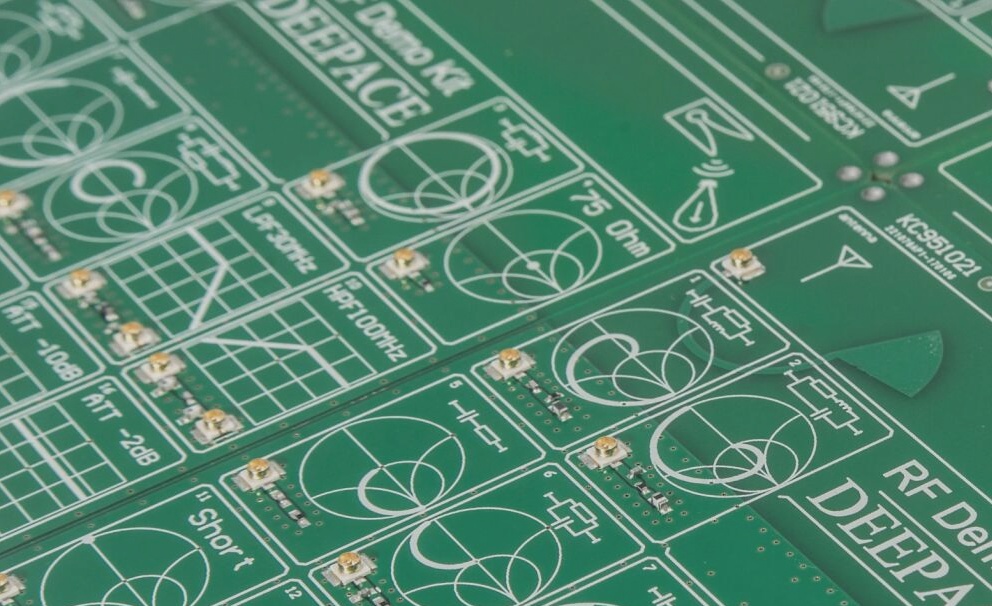
This article introduces EMI control technology in digital circuit PCB board design. With the improvement of IC device integration and the gradual miniaturization of equipment, alongside increasing device speeds, the issue of EMI in electronic products is becoming more severe. From the perspective of EMC/EMI design for system equipment, addressing EMC/EMI issues during the PCB board design phase is an effective and economical approach to ensuring that the system equipment meets electromagnetic compatibility standards.
1. Principles of EMI Generation and Suppression
EMI originates from sources of electromagnetic interference that transfer energy to sensitive systems through coupling paths. It manifests in three primary forms: conduction through wires or common grounds, radiation through space, or coupling via near-field. EMI hazards include degradation of transmission signal quality, interference, or even damage to circuits or equipment, thereby potentially preventing compliance with specified technical indices in electromagnetic compatibility standards. To mitigate EMI, digital circuit EMI design should adhere to the following principles: decompose relevant EMC/EMI technical specifications into individual circuit boards and control them in stages. Addressing the three elements of EMI—interference sources, energy coupling paths, and sensitive systems—ensures a flat frequency response in circuits and guarantees normal, stable circuit operation. Initiating with equipment front-end design, emphasizing EMC/EMI considerations can reduce overall design costs.

2. EMI control technology of digital circuit PCB board
When dealing with various forms of EMI, specific problems must be analyzed. In the PCB board design of digital circuits, EMI control can be carried out from the following aspects.
2.1 Device Selection
In EMI design, the first consideration should be the speed of the selected device. Replacing a device with a 5ns rise time with one having a 2.5ns rise time can increase EMI by a factor of about 4. EMI radiated intensity is proportional to the square of the frequency, and the EMI frequency (fknee), also known as the EMI emission bandwidth, is a function of the signal rise time (Tr) rather than the signal frequency: fknee = 0.35/Tr. The frequency range for this type of radiated EMI is 30MHz to several GHz. In this frequency band, even very short traces on a PCB can act as transmitting antennas, potentially disrupting circuit function. Therefore, in device selection, while meeting circuit performance requirements, it is advisable to use lower-speed chips and appropriate driving/receiving circuits. Additionally, the packaging form of the device significantly affects signal integrity in high-speed designs due to parasitic inductance and capacitance of lead pins. Surface-mount device (SMD) packages generally exhibit smaller parasitic parameters compared to through-hole packages, and ball grid array (BGA) packages typically have smaller parasitics than quad flat pack (QFP) packages.
2.2 Connector Selection and Signal Terminal Definition
Connectors are critical for high-speed signal transmission and are prone to EMI issues. When designing connector terminals, increasing the number of ground pins can minimize the distance between the signal and ground, thereby reducing the effective signal loop area that generates radiation within the connector. This setup also provides a low-impedance return path. If necessary, isolating key signals with ground pins should be considered.
2.3 Laminate Design
If cost allows, increasing the number of ground layers and placing signal layers adjacent to ground plane layers can reduce EMI radiation. For high-speed PCBs, close coupling of power and ground planes helps reduce power supply impedance, thus mitigating EMI.
2.4 Layout
A rational layout based on signal current flow minimizes interference between signals. Effective layout principles include segregating analog signals from digital signals, keeping clock lines away from sensitive circuits with minimal trace lengths, and avoiding central placement of power dissipation circuits to manage heat dissipation and radiation. Connectors should ideally be positioned on one side of the board, away from high-frequency circuits. Input/output circuits should be placed near corresponding connectors, with decoupling capacitors situated close to power supply pins. Careful consideration should also be given to power division feasibility, ensuring multi-power devices are placed across power division boundaries to reduce plane division impact on EMI. Maintain continuous return paths.
2.5 Wiring
Impedance control is crucial for high-speed signal lines to prevent signal reflection, overshoot, ringing, and EMI radiation. Segment signals based on EMI radiation intensity and sensitivity (analog signals, clock signals, I/O signals, buses, power supplies, etc.) to minimize coupling. Control trace length, number of vias, cross partitions, terminations, routing layers, and return paths, especially for high-speed clock signals. Ensure critical signals do not cross segmented areas. Tight coupling of high-speed differential signal traces is essential. Compliance with stripline and microstrip line requirements with their respective reference planes is also necessary. Keep decoupling capacitor leads short and wide. Maintain distance of all signal traces from board edges. Employ appropriate topology for multi-point connection networks to reduce signal reflections and EMI emissions.
2.6 Split Processing of Power Plane
When dividing power supply layers, ensure continuity and sufficient copper foil width for each sub-power supply area. Keep division lines narrow (20-50 mils) to minimize radiation gaps. Maintain ground plane layer integrity; if division is necessary, separate digital, analog, and noise grounds, connecting them externally through a common ground point to reduce fringe radiation of the power supply. Follow the 20H design principle, where the ground plane size exceeds the power plane by 20 times its height, reducing fringing field radiation intensity by 70%.
3. Other Control Methods for EMI
3.1 Power System Design
Design a low-impedance power system to ensure power distribution system impedance in the sub-fknee frequency range is lower than the target impedance. Use filters for conducted interference control. Implement effective power supply decoupling with suitable decoupling capacitors to enhance device reliability and reduce high-frequency noise in the power supply, thereby minimizing EMI.
3.2 Grounding
Grounding design is critical for overall board EMI reduction. Utilize single-point grounding, multi-point grounding, or mixed grounding as necessary. Separate digital, analog, and noise grounds, establishing an appropriate common ground point. In double-sided designs without a ground layer, design the ground grid meticulously, ensuring ground trace width exceeds that of power traces and signal traces. Alternatively, employ large-area ground planes, ensuring continuous grounding on the same layer for improved impedance reduction in multi-layer board designs.
3.3 Series Damping Resistor
Introduce small series resistors (typically 22-33Ω) at key signal outputs, if circuit timing allows. This approach slows rise/fall times, smooths overshoot and undershoot signals, reduces high-frequency harmonic amplitude of output waveforms, and effectively suppresses EMI.
3.4 Shielding
Implement EMI shielding materials or shielding mesh for critical components and signals. Shield key signals with strip lines or isolate them with ground traces on both sides to minimize EMI.
3.5 Spread Spectrum
Spread spectrum techniques modulate signals to broaden signal energy across a wider frequency range, effectively reducing EMI. Controlled modulation of clock signals can significantly decrease emissions (by 7 to 20 dB) without substantial clock signal jitter.
3.6 EMI Analysis and Testing
After PCB board wiring, use EMI simulation software and systems to analyze EMC/EMI environments, assessing compliance with relevant electromagnetic compatibility standards. Perform scanning tests using electromagnetic radiation scanners post-assembly and power-on to map electromagnetic field distributions on the PCB, optimizing PCB board design based on test results.
4. Summary
With advancing high-speed chip technologies and shrinking PCB sizes, PCB board designs face increasingly challenging EMI issues. Continuous exploration and innovation are essential for successful EMC/EMI design in PCB boards.
1. Principles of EMI Generation and Suppression
EMI originates from sources of electromagnetic interference that transfer energy to sensitive systems through coupling paths. It manifests in three primary forms: conduction through wires or common grounds, radiation through space, or coupling via near-field. EMI hazards include degradation of transmission signal quality, interference, or even damage to circuits or equipment, thereby potentially preventing compliance with specified technical indices in electromagnetic compatibility standards. To mitigate EMI, digital circuit EMI design should adhere to the following principles: decompose relevant EMC/EMI technical specifications into individual circuit boards and control them in stages. Addressing the three elements of EMI—interference sources, energy coupling paths, and sensitive systems—ensures a flat frequency response in circuits and guarantees normal, stable circuit operation. Initiating with equipment front-end design, emphasizing EMC/EMI considerations can reduce overall design costs.

2. EMI control technology of digital circuit PCB board
When dealing with various forms of EMI, specific problems must be analyzed. In the PCB board design of digital circuits, EMI control can be carried out from the following aspects.
2.1 Device Selection
In EMI design, the first consideration should be the speed of the selected device. Replacing a device with a 5ns rise time with one having a 2.5ns rise time can increase EMI by a factor of about 4. EMI radiated intensity is proportional to the square of the frequency, and the EMI frequency (fknee), also known as the EMI emission bandwidth, is a function of the signal rise time (Tr) rather than the signal frequency: fknee = 0.35/Tr. The frequency range for this type of radiated EMI is 30MHz to several GHz. In this frequency band, even very short traces on a PCB can act as transmitting antennas, potentially disrupting circuit function. Therefore, in device selection, while meeting circuit performance requirements, it is advisable to use lower-speed chips and appropriate driving/receiving circuits. Additionally, the packaging form of the device significantly affects signal integrity in high-speed designs due to parasitic inductance and capacitance of lead pins. Surface-mount device (SMD) packages generally exhibit smaller parasitic parameters compared to through-hole packages, and ball grid array (BGA) packages typically have smaller parasitics than quad flat pack (QFP) packages.
2.2 Connector Selection and Signal Terminal Definition
Connectors are critical for high-speed signal transmission and are prone to EMI issues. When designing connector terminals, increasing the number of ground pins can minimize the distance between the signal and ground, thereby reducing the effective signal loop area that generates radiation within the connector. This setup also provides a low-impedance return path. If necessary, isolating key signals with ground pins should be considered.
2.3 Laminate Design
If cost allows, increasing the number of ground layers and placing signal layers adjacent to ground plane layers can reduce EMI radiation. For high-speed PCBs, close coupling of power and ground planes helps reduce power supply impedance, thus mitigating EMI.
2.4 Layout
A rational layout based on signal current flow minimizes interference between signals. Effective layout principles include segregating analog signals from digital signals, keeping clock lines away from sensitive circuits with minimal trace lengths, and avoiding central placement of power dissipation circuits to manage heat dissipation and radiation. Connectors should ideally be positioned on one side of the board, away from high-frequency circuits. Input/output circuits should be placed near corresponding connectors, with decoupling capacitors situated close to power supply pins. Careful consideration should also be given to power division feasibility, ensuring multi-power devices are placed across power division boundaries to reduce plane division impact on EMI. Maintain continuous return paths.
2.5 Wiring
Impedance control is crucial for high-speed signal lines to prevent signal reflection, overshoot, ringing, and EMI radiation. Segment signals based on EMI radiation intensity and sensitivity (analog signals, clock signals, I/O signals, buses, power supplies, etc.) to minimize coupling. Control trace length, number of vias, cross partitions, terminations, routing layers, and return paths, especially for high-speed clock signals. Ensure critical signals do not cross segmented areas. Tight coupling of high-speed differential signal traces is essential. Compliance with stripline and microstrip line requirements with their respective reference planes is also necessary. Keep decoupling capacitor leads short and wide. Maintain distance of all signal traces from board edges. Employ appropriate topology for multi-point connection networks to reduce signal reflections and EMI emissions.
2.6 Split Processing of Power Plane
When dividing power supply layers, ensure continuity and sufficient copper foil width for each sub-power supply area. Keep division lines narrow (20-50 mils) to minimize radiation gaps. Maintain ground plane layer integrity; if division is necessary, separate digital, analog, and noise grounds, connecting them externally through a common ground point to reduce fringe radiation of the power supply. Follow the 20H design principle, where the ground plane size exceeds the power plane by 20 times its height, reducing fringing field radiation intensity by 70%.
3. Other Control Methods for EMI
3.1 Power System Design
Design a low-impedance power system to ensure power distribution system impedance in the sub-fknee frequency range is lower than the target impedance. Use filters for conducted interference control. Implement effective power supply decoupling with suitable decoupling capacitors to enhance device reliability and reduce high-frequency noise in the power supply, thereby minimizing EMI.
3.2 Grounding
Grounding design is critical for overall board EMI reduction. Utilize single-point grounding, multi-point grounding, or mixed grounding as necessary. Separate digital, analog, and noise grounds, establishing an appropriate common ground point. In double-sided designs without a ground layer, design the ground grid meticulously, ensuring ground trace width exceeds that of power traces and signal traces. Alternatively, employ large-area ground planes, ensuring continuous grounding on the same layer for improved impedance reduction in multi-layer board designs.
3.3 Series Damping Resistor
Introduce small series resistors (typically 22-33Ω) at key signal outputs, if circuit timing allows. This approach slows rise/fall times, smooths overshoot and undershoot signals, reduces high-frequency harmonic amplitude of output waveforms, and effectively suppresses EMI.
3.4 Shielding
Implement EMI shielding materials or shielding mesh for critical components and signals. Shield key signals with strip lines or isolate them with ground traces on both sides to minimize EMI.
3.5 Spread Spectrum
Spread spectrum techniques modulate signals to broaden signal energy across a wider frequency range, effectively reducing EMI. Controlled modulation of clock signals can significantly decrease emissions (by 7 to 20 dB) without substantial clock signal jitter.
3.6 EMI Analysis and Testing
After PCB board wiring, use EMI simulation software and systems to analyze EMC/EMI environments, assessing compliance with relevant electromagnetic compatibility standards. Perform scanning tests using electromagnetic radiation scanners post-assembly and power-on to map electromagnetic field distributions on the PCB, optimizing PCB board design based on test results.
4. Summary
With advancing high-speed chip technologies and shrinking PCB sizes, PCB board designs face increasingly challenging EMI issues. Continuous exploration and innovation are essential for successful EMC/EMI design in PCB boards.


