PCB Wiring Essentials: Tips for Effective Layout Design
Understanding PCB Layers and Hole Types
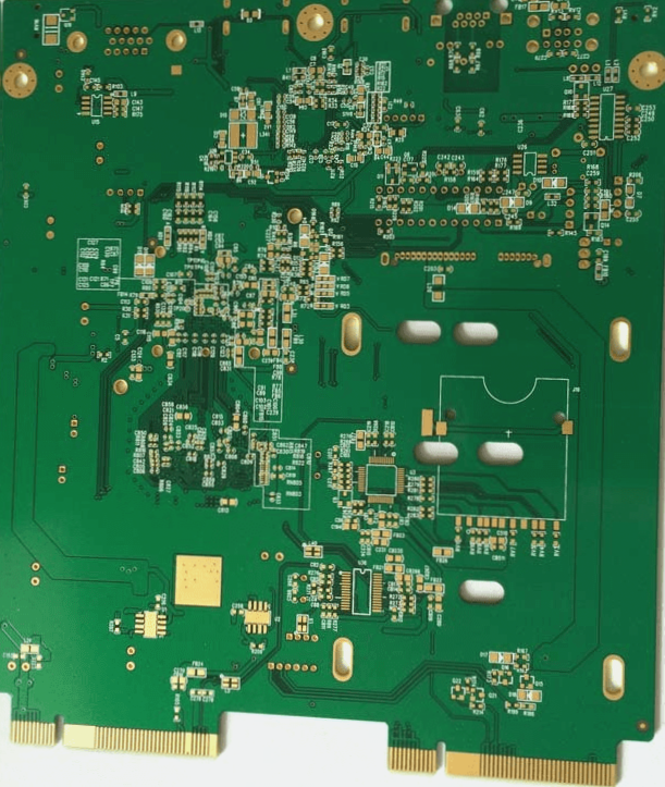
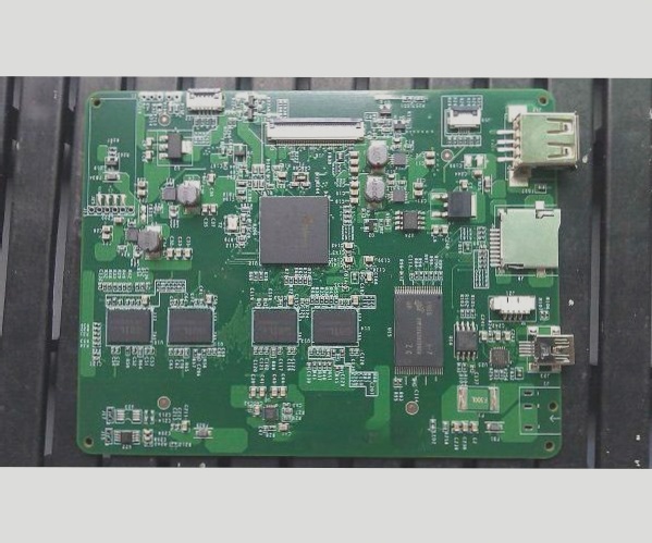
When it comes to PCB design, understanding the different layers and hole types is crucial. PCB layers can be single-layer, double-layer, or multi-layer, with multi-layer boards being ideal for high component density. Through-holes, blind holes, and buried holes serve different purposes in connecting components.
Precautions for Wiring High-Demand Lines
Before automatic wiring, it’s essential to prepare for high-demand interactive lines. Keeping input and output lines separate, using ground cables for isolation, and organizing wiring rules are key steps to ensure efficient wiring.
Layout Design Guidelines
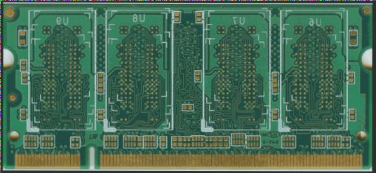
When designing the layout, it’s important to keep digital and analog circuits separate and consider the distance between low-speed and high-speed lines. Segregating digital and analog grounding is fundamental to prevent interference and noise issues.
Wiring Precautions:
- Use decoupling capacitors between power supply and ground wires.
- Widen ground wires more than power lines.
- Utilize a large copper area as ground.
Mixing Digital and Analog Circuits:
For PCBs with both digital and analog circuits, careful routing is necessary to minimize interference. Separate the grounds of digital and analog circuits within the board and connect them at a single point.
Managing Line Corners:
Line corners play a crucial role in signal integrity. Avoid right angles and opt for 45-degree angles or rounded corners to reduce reflection issues, especially for sensitive lines.
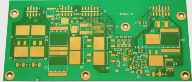
Design Rule Checks Post-Routing:
- Verification is crucial after completing any task. It is similar to reviewing exam answers to ensure high-quality PCB designs.
- Key Inspection Aspects:
- Verify reasonable distances between lines, component pads, through-holes, and meet production requirements.
- Assess appropriate widths of power and ground cables, ensure tight coupling (low wave impedance), and check space to widen ground cables.
- Confirm protective measures for key signal lines, ensuring clear separation of input and output lines.
- Ensure independent ground wires for analog and digital circuits.
- Check for any graphics (icons, notations) that may cause signal shorts.
- Modify unsatisfactory lines.
- Verify process line adherence on the PCB, ensuring resistance welding meets production requirements and preventing character marks from compromising electric quality.
- Check for reduced edge frames in multi-layer boards to avoid exposed copper foil leading to shorts on the power supply layer.
- Importance:
These skills and methods are essential in PCB design. Apart from using tools proficiently, a strong theoretical base and practical experience are vital for efficient layout. Caution is key; every wiring and layout step must be taken seriously as a small error can result in a defective final product. Investing time in meticulous detail checks during the design phase is preferable to addressing errors later, which could consume more time. Attention to detail is crucial in PCB design.