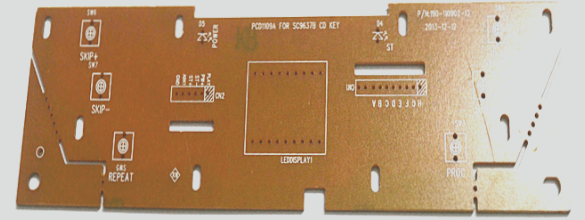
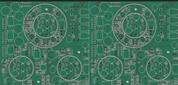
1. As the carrier of various components and the hub of circuit signal transmission, the PCB board has become a crucial part of electronic information products. Its quality and reliability significantly influence the entire equipment’s performance.

2. However, due to cost and technical constraints, numerous failure issues arise during the production and application of PCB boards.

3. To address these challenges, it is essential to employ established failure analysis techniques to ensure the quality and reliability of PCB boards during manufacturing.

4. This article presents a summary of ten commonly used failure analysis techniques for reference.

1. Visual inspection

Visual inspection involves visually or using simple instruments like a stereo microscope, metallographic microscope, or magnifying glass to identify PCB board failures and related physical evidence. Its primary function is to pinpoint failures and initially determine failure modes. Appearance inspection checks for PCB contamination, corrosion, board breakage locations, circuit wiring irregularities, and patterns of failures, whether batch-related or isolated to specific areas. Many failures are discovered only post-assembly of PCB board A, necessitating scrutiny of assembly processes and materials to assess their role in causing failures.

2. X-ray fluoroscopy

X-ray fluoroscopy examines parts inaccessible to visual inspection and internal defects within PCB through-holes. This system exploits varying material densities or thicknesses to image via X-ray absorption or transmission principles. It primarily detects internal defects of solder joints, through-holes, and faulty BGA or CSP device soldering in high-density packages. Industrial X-ray fluoroscopy achieves sub-micron resolutions and is transitioning from 2D to 3D imaging. Though 5D systems exist, they are costly and rarely applied in industry.

3. Slice analysis

Slice analysis involves obtaining PCB cross-sectional structures via sampling, embedding, slicing, polishing, corrosion, and observation. It provides detailed microstructure insights (e.g., through-holes, plating quality), crucial for improving PCB quality. However, it’s destructive and necessitates skilled technicians due to time-consuming sample preparation. Detailed processes are outlined in IPC standards IPC-TM-650 2.1.1 and IPC-MS-810.

4. Scanning acoustic microscope

Scanning acoustic microscopes, especially C-mode ultrasonic types, analyze electronic packaging or assembly. They use high-frequency ultrasound reflections to image material interfaces based on amplitude, phase, and polarity changes. This method detects PCB and PCB board A defects like cracks, delamination, inclusions, and voids, crucial in assessing lead-free process challenges. Their advantage lies in non-destructive testing of multi-layer high-density PCBs.

5. Micro-infrared analysis

Micro-infrared analysis combines infrared spectroscopy and microscopy to analyze organic material absorption differences. It identifies trace organic contaminants affecting PCB pad or lead pin solderability, crucial for resolving process issues in electronic technology.

6. Scanning electron microscope analysis

Scanning electron microscopes (SEM) are pivotal for failure analysis due to their high-resolution imaging capabilities. SEM observes pad topography, solder joint metallography, intermetallic compounds, and tin whisker growth, crucial for assessing solderability. Unlike optical microscopes, SEM produces monochrome images and requires conductive samples or surface coating for non-conductive materials.

7. X-ray energy spectrum analysis

X-ray energy spectrum analysis, often paired with SEM, identifies elements via characteristic X-ray emissions from bombarded sample surfaces. It’s useful for analyzing PCB pad surface components and contaminants affecting solderability. While energy spectrometers provide rapid analysis, their quantitative accuracy for elements below 0.1% is limited.

8. Photoelectron spectroscopy (XPS) analysis

XPS analyzes surface element chemistry via X-ray-induced electron emissions, offering insights into PCB coating quality, pollutants, and oxidation. It’s non-destructive and excels in multi-layer elemental depth profiling, offering higher sensitivity than energy spectrometry.

9. Thermal analysis differential scanning calorimetry (DSC)

DSC measures material thermal and thermodynamic properties via heat flow differences relative to temperature or time. It assesses polymer curing and glass transition temperatures critical for PCB reliability.

10. Thermomechanical Analyzer (TMA)

TMA evaluates material deformations under thermal or mechanical stress. It measures linear expansion coefficients and glass transition temperatures in PCB substrates, crucial for preventing metallized hole fractures post-soldering.

Understanding these analysis techniques aids in comprehending PCB failure mechanisms, enhancing quality control to preempt future issues effectively.

Leave a Comment

Contact

WellCircuits
More than PCB

Upload your GerberFile(7z,rar,zip)