When the length of a single-sided double-contact FPC electrode exceeds 3.0mm and its width is below 0.3mm, it is prone to deformation, distortion, and fracture during the manufacturing process (including etching, film removal, surface cleaning, and applying protective film), which significantly impacts the product’s yield rate. For instance, an FPC company previously handled such an order using standard procedures, resulting in a low yield rate of approximately 50%, making delivery impossible. However, following process enhancements, the yield rate improved to between 90% and 95%. Below, I will outline the strategies for process improvement:
1. Starting point for process improvement:

1. As illustrated in Figure 1, we consider part B as the section that requires hollowing during the process (following the etching of the upper protective film). When this section is hollowed out, it lacks any reinforced support for the hollowed electrode, which may lead to twisting, deformation, or breakage due to external forces (such as the spray pressure from the leveling machine, retraction, and transport). Thus, the critical aspect of process enhancement is to establish support for the delicate electrode.
2. Support Selection: Since the support is utilized from the pre-etching phase to the application of the upper protective film—particularly requiring hot pressing—we must select materials capable of enduring high temperatures. High-temperature tape is suitable in this case. The tape must ensure no adhesive transfer and exhibit heat-resistant properties (rapid press) at elevated temperatures.
3. Process Overview: The circuit is fabricated using a wet film; the B-side is first silk-screened, followed by the A-side after baking, and then baked again. Exposure and development follow, with a crucial note that side B should not be exposed, as this complicates film removal. After development, tape is applied to side B. It’s important that the high-temperature tape lies flat, and if there’s a reinforced alignment mark, the tape should ideally not extend beyond this marking line, as pressing may leave slight impressions at the high-temperature tape’s position. If reinforcement is present, it can cover any indentations. Normal procedures for etching, developing, and surface cleaning continue, followed by the pressing of the upper protective film, for which parameters must be optimized. The optimization principle involves using minimal time, pressure, and temperature, as excessive heat, prolonged duration, or high pressure may lead to adhesive transfer and complicate the removal of the wet film underneath. After removing the high-temperature tape and film, the board is ground to eliminate any ashing copper at the electrode; baking follows to cure the upper protective film, while subsequent steps remain unchanged.
4. Conclusion: This method can be somewhat more complex and requires additional high-temperature tape as auxiliary materials. However, I believe it is highly suitable for producing single-sided, double-contact FPCs with electrode lengths greater than 3.0 mm and widths less than 0.3 mm, positively impacting yield improvements. Feel free to experiment if you’re interested and assess the advantages and disadvantages for yourself.
1. Starting point for process improvement:
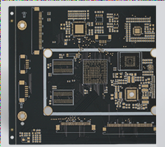
1. As illustrated in Figure 1, we consider part B as the section that requires hollowing during the process (following the etching of the upper protective film). When this section is hollowed out, it lacks any reinforced support for the hollowed electrode, which may lead to twisting, deformation, or breakage due to external forces (such as the spray pressure from the leveling machine, retraction, and transport). Thus, the critical aspect of process enhancement is to establish support for the delicate electrode.
2. Support Selection: Since the support is utilized from the pre-etching phase to the application of the upper protective film—particularly requiring hot pressing—we must select materials capable of enduring high temperatures. High-temperature tape is suitable in this case. The tape must ensure no adhesive transfer and exhibit heat-resistant properties (rapid press) at elevated temperatures.
3. Process Overview: The circuit is fabricated using a wet film; the B-side is first silk-screened, followed by the A-side after baking, and then baked again. Exposure and development follow, with a crucial note that side B should not be exposed, as this complicates film removal. After development, tape is applied to side B. It’s important that the high-temperature tape lies flat, and if there’s a reinforced alignment mark, the tape should ideally not extend beyond this marking line, as pressing may leave slight impressions at the high-temperature tape’s position. If reinforcement is present, it can cover any indentations. Normal procedures for etching, developing, and surface cleaning continue, followed by the pressing of the upper protective film, for which parameters must be optimized. The optimization principle involves using minimal time, pressure, and temperature, as excessive heat, prolonged duration, or high pressure may lead to adhesive transfer and complicate the removal of the wet film underneath. After removing the high-temperature tape and film, the board is ground to eliminate any ashing copper at the electrode; baking follows to cure the upper protective film, while subsequent steps remain unchanged.
4. Conclusion: This method can be somewhat more complex and requires additional high-temperature tape as auxiliary materials. However, I believe it is highly suitable for producing single-sided, double-contact FPCs with electrode lengths greater than 3.0 mm and widths less than 0.3 mm, positively impacting yield improvements. Feel free to experiment if you’re interested and assess the advantages and disadvantages for yourself.

