It is evident that direct chip attachment on PWBs significantly reduces the packaging efficiency of such assemblies, unless components can be mounted on both sides of the PWB substrate. Studies have demonstrated that wire bonding can be accomplished on both sides of a PWB with special fixturing, and outer lead bonding (OLB) of TABs can also be performed on both sides of the PWB substrate. Thus, while single-sided bare chip assembly on PWBs decreases packaging efficiency to approximately half that of other substrate constructions, the capability to place components on both sides of PWBs restores it to the same packaging efficiency level as others.
The ongoing enhancement in component performance and PCB lead density, coupled with the shrinking of package sizes, necessitates that PWB technology explore methods to elevate the interconnection density of the substrate. With the advent and ongoing advancement of packaging techniques such as ball grid array (BGA), chip-scale packaging (CSP), and chip-on-board (COB), traditional PWB technology has reached a juncture where alternative approaches for achieving high-density interconnection must be devised.

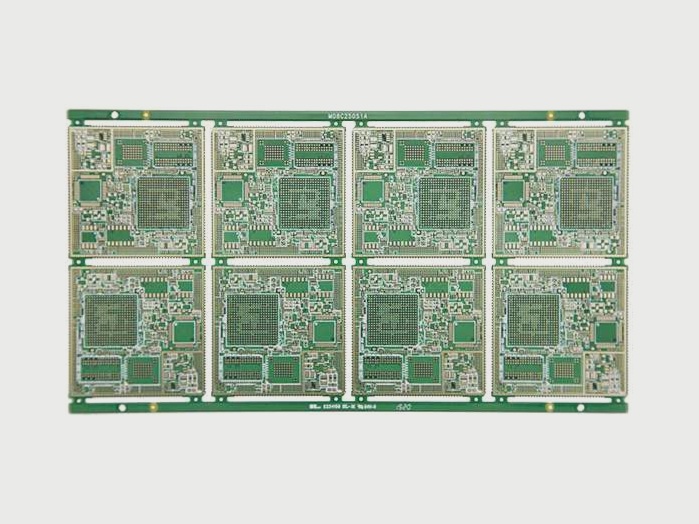
Image 1: 10 Layer HDI rigid flex PCB
This approach is the most direct solution: when existing layers lack sufficient space for all required interconnections, adding a layer becomes necessary. While this method has been widely adopted in the past, the cost-effectiveness of substrates now demands a meticulous design analysis to minimize layer counts in MLBs, as each additional layer significantly escalates board costs. For instance, when assessing 6- × 8-inch MLBs manufactured in high volumes, maintaining consistent yields and conductor density reveals a nearly linear correlation between board expenses and layer count.
In boards operating at frequencies that necessitate transmission line characteristics, any increase in signal layers effectively doubles the total layer count. This stems from the imperative to alternate ground or DC power planes among signal planes. Consequently, manufacturing yields invariably decline with an escalation in layer numbers across all linewidth categories. Such scenarios are commonplace in board fabrication, where heightened complexity and increased MLB thickness due to additional layers frequently contribute to heightened production floor challenges.

Certainly! Here’s the revised version of the text:
—
There are three basic ways to increase PCB density and enhance connectivity or available conductor capacity:
1. Reduce hole and pad diameters. For more information, refer to the previous blog.
2. Increase the number of conductive channels between pads by reducing conductor widths.
3. Increase the number of signal planes.
The impact of each approach on PCB manufacturing yields and onboard costs will be discussed sequentially. It should be noted that the last option is the simplest but also the most costly solution. Therefore, it should only be considered when methods for addressing the first two conditions are proven inadequate for achieving the desired board density.

Certainly! Here’s a polished version of your text:
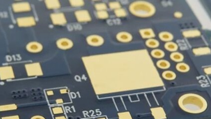
Image 3: 8-layer High-Density PCB Supplier
The ongoing enhancement in component performance and PCB lead density, coupled with the shrinking of package sizes, necessitates that PWB technology explore methods to elevate the interconnection density of the substrate. With the advent and ongoing advancement of packaging techniques such as ball grid array (BGA), chip-scale packaging (CSP), and chip-on-board (COB), traditional PWB technology has reached a juncture where alternative approaches for achieving high-density interconnection must be devised.

Image 1: 10 Layer HDI rigid flex PCB
This approach is the most direct solution: when existing layers lack sufficient space for all required interconnections, adding a layer becomes necessary. While this method has been widely adopted in the past, the cost-effectiveness of substrates now demands a meticulous design analysis to minimize layer counts in MLBs, as each additional layer significantly escalates board costs. For instance, when assessing 6- × 8-inch MLBs manufactured in high volumes, maintaining consistent yields and conductor density reveals a nearly linear correlation between board expenses and layer count.
In boards operating at frequencies that necessitate transmission line characteristics, any increase in signal layers effectively doubles the total layer count. This stems from the imperative to alternate ground or DC power planes among signal planes. Consequently, manufacturing yields invariably decline with an escalation in layer numbers across all linewidth categories. Such scenarios are commonplace in board fabrication, where heightened complexity and increased MLB thickness due to additional layers frequently contribute to heightened production floor challenges.

Certainly! Here’s the revised version of the text:
—
There are three basic ways to increase PCB density and enhance connectivity or available conductor capacity:
1. Reduce hole and pad diameters. For more information, refer to the previous blog.
2. Increase the number of conductive channels between pads by reducing conductor widths.
3. Increase the number of signal planes.
The impact of each approach on PCB manufacturing yields and onboard costs will be discussed sequentially. It should be noted that the last option is the simplest but also the most costly solution. Therefore, it should only be considered when methods for addressing the first two conditions are proven inadequate for achieving the desired board density.

Certainly! Here’s a polished version of your text:
Image 3: 8-layer High-Density PCB Supplier


