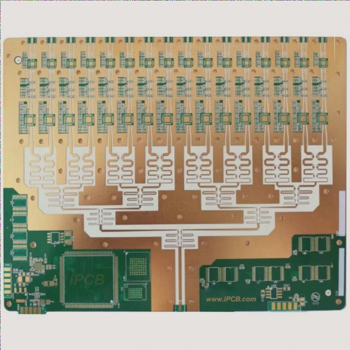
I have a board designed in Diptrace. I want to use the front of the board as a user interface. I would like to make it a bit fancy, so I would like to place artwork on the copper and solder mask layer as well.
Diptrace has a feature to import bitmaps, which works ok on the silk layer and acceptable on the copper. However it doesn’t seem to do anything on the solder mask layer. I wouldn’t mind tracing over the solder mask manually using the polygon tool, but the render in the PCB Layout software is a very crude low resolution version, it’s a pain to do so.
Another trick I tried was to add a custom footprint and import the artwork from a DXF file, but it seems that file format isn’t that well supported and the result was a glitchy mess with text not rendering (I used Inkscape to draw the artwork).
Next I tried to export the board as gerber and import it in Kicad. I’m a bit surprised it actually sort of worked, but it messes up the paths of all components. All pads are suddenly converted to through hole. I also tried exporting to P-CAD and opening that in Kicad, but that seems to mess up the copper pours.
Another thing I’ll try is to convert the gerbers to svg or something, but I haven’t yet found a tool that could do the reverse.
More ideas are very welcome.


