Using ENIG Surface Finish for 4 Layer PCB: Post-Assembly Testing Considerations
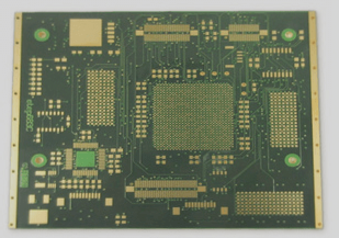
Hello everyone, I am currently working on a 4-layer PCB with ENIG surface finish, specifically for QFN components. I have incorporated small circular pads for post-assembly testing purposes. One dilemma I am facing is whether it is more beneficial to leave the pad with or without a stencil opening for solder paste application.
When considering leaving the pad uncovered, concerns arise regarding the potential impact on track reliability. Factors such as oxidation and corrosion come into play. While gold is generally known for its stability, reports of black pad issues with ENIG raise questions about its reliability in this context.
On the other hand, covering the pad raises a different set of considerations. The presence of flux residue could potentially hinder conductivity between the probe and pad, leading to false test failures. However, this approach may be preferred over risking reliability issues.
Given these factors, the choice between leaving the pad exposed or covered poses a crucial decision point, especially when using leaded no-clean solder paste. Your recommendations and insights on this matter would be greatly appreciated. Thank you!