Everyone is aware of the methods to prevent PCB bending and warping during reflow furnace processing. Here’s a detailed explanation for everyone:
1. Minimize the Impact of Temperature on PCB Stress
Since “temperature” is the primary contributor to board stress, lowering the reflow oven temperature or reducing the rate of heating and cooling for the board can significantly decrease the likelihood of bending and warping. However, be cautious, as this might lead to other issues, such as solder short circuits.
2. Utilize High Tg Materials
Tg, or glass transition temperature, refers to the temperature at which a material transitions from a glassy state to a rubbery state. Materials with lower Tg values soften more quickly upon entering the reflow furnace, and the duration before they reach a rubbery state is also extended, leading to greater deformation. Employing higher Tg materials enhances the board’s ability to withstand stress and deformation, though they tend to be more expensive.
3. Increase Circuit Board Thickness
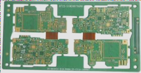
1. In PCB board manufacturing, to achieve lighter and thinner designs for various electronic products, board thicknesses have been reduced to 1.0mm, 0.8mm, or even 0.6mm. Maintaining structural integrity after passing through the reflow furnace at these thicknesses can be quite challenging. It is advisable that if there are no specific requirements for weight and thinness, a board thickness of 1.6mm should be used, as this significantly lowers the risk of bending and deformation.
2. Minimize the size of the circuit board and reduce the number of panels.
Since most reflow furnaces use chains to move the circuit boards forward, larger board sizes can lead to issues such as denting and deformation due to their weight. To mitigate this, orient the long side of the circuit board along the edge of the reflow furnace chain. This alignment helps minimize the impact of the board’s weight, thereby reducing potential depressions and deformations. Additionally, decreasing the number of panels follows this logic; using the narrow edge to pass through the furnace can further lessen deformation.
3. Utilize furnace tray fixtures.
If the aforementioned strategies are impractical, consider using reflow carriers or templates to help reduce deformation. These carriers assist in minimizing bending by supporting the circuit board during thermal expansion and contraction. Ideally, the tray should hold the board until its temperature drops below the Tg value, allowing it to solidify while maintaining its shape.
4. If a single-layer tray does not adequately minimize PCB deformation, adding a second layer to sandwich the circuit board between upper and lower pallets can significantly alleviate deformation issues during reflow. However, this solution can be costly and requires manual handling and recycling of the trays.
5. Use routing instead of V-Cut for sub-boards.
Since V-Cut techniques can compromise the structural integrity of the panel between circuit boards, it is advisable to avoid V-Cut for creating sub-boards or to reduce the depth of the V-Cut if necessary.
If you have any PCB manufacturing needs, please do not hesitate to contact me.Contact me

