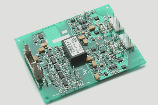
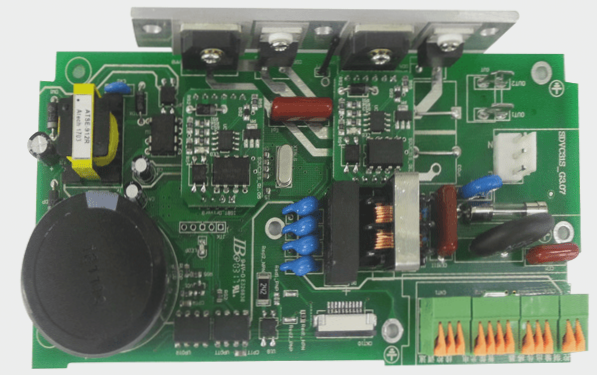
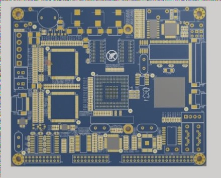
The Importance of PCB Layout and Device Placement
- 1. Achieving success with a product heavily relies on the layout of printed circuit boards (PCBs) and how devices are positioned. It is crucial to focus on both internal quality and overall aesthetics. A balanced and uncluttered arrangement of components is key, avoiding overcrowding and uneven distribution. Minimize the use of vias and aim for a rectangular board shape with a 3:2 or 4:3 aspect ratio. Opting for multi-layer boards can significantly enhance performance and signal integrity.
- 2. PCBs are typically divided into analog circuits (sensitive to interference), digital circuits (susceptible to interference and generating interference), and power drive circuits (potential sources of interference). Proper segmentation into these areas is vital to reduce interference and optimize performance.
- 3. Select components with low power consumption and high stability. Minimize the use of high-speed devices to decrease noise and improve reliability.
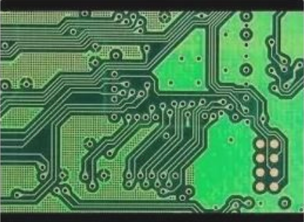
- 4. Pay close attention to routing: avoid thin traces for wide lines, ensure smooth paths for high-voltage and high-frequency lines, and eliminate sharp corners and right angles. Wide ground traces with ample copper areas enhance connectivity.
- 5. External clocks can introduce high-frequency noise, impacting system performance and electromagnetic compatibility. Opt for low-frequency microcontrollers to reduce noise. Recent technologies like internal phase-locked loops have reduced external clock requirements while maintaining computing speed.
- 6. Logical routing directions are crucial to prevent interference. Separate input/output, AC/DC, strong/weak signals, high/low frequencies, and voltages. Linear or separated routing paths are preferred over circular patterns. Vertical routing between layers is generally recommended.
- 7. Device placement is key for noise mitigation. Group related devices together, especially noise-prone components like clock generators and CPU inputs. Segregate noise-sensitive circuits from logic circuits and consider separate boards if needed to minimize interference.
Ground Wire Technology and Electromagnetic Compatibility
- 1. Analog and digital circuits have different wiring requirements. In analog circuits, even small noise voltages can distort output signals due to amplification. Digital circuits have higher noise tolerance. Proper power supply and ground bus selection is crucial for instrument reliability.
- 2. Keep digital and analog grounds separate or connect at one point with widened ground wires. Thicker wires are better for higher currents. Prioritize wire width: Ground wire > power wire > signal wire.
- 3. Place power and ground lines close together in a “well” shape on the PCB for balanced current distribution.
- 4. Increase line distance to reduce crosstalk if needed. Use zero-volt lines for isolation between signals. Decoupling, filtering, and isolation are key measures for hardware anti-interference, especially between input and output signals.
Decoupling, filtering, and isolation are vital for hardware anti-interference.
PCB Power Input and Filtering Guidelines
- Power Input: Connect the power input end across an electrolytic capacitor of 10~100uF. It is recommended to use more than 100uF if possible. Additionally, each integrated circuit chip should have a 0.01uF ceramic capacitor. For devices with weak anti-noise ability and significant power changes when turned off, such as RAM and ROM storage devices, a decoupling capacitor should be directly connected between the power line and the ground line of the chip.
- Filtering: Filtering involves categorizing signals based on their frequency characteristics and managing their flow. Common filters include low-pass filters, high-pass filters, and band-pass filters. Low-pass filters are utilized on the incoming AC power line to allow smooth passage of the 50-cycle AC power while diverting high-frequency noises to the ground. The effectiveness of a low-pass filter is measured by its insertion loss. It is crucial to select a low-pass filter with an appropriate insertion loss to suppress noise without compromising system safety. High-pass and band-pass filters should be chosen based on the system’s signal processing requirements.
- Signal Isolation: Optoelectronic isolation, particularly optical isolation, is a typical method of signal isolation. Optoelectronic isolation devices are employed to separate the input and output of single-chip microcomputers. This approach prevents interference signals from entering the system and ensures that the system’s internal noise is not conducted. Shielding, such as using metal boxes, is effective in isolating components with high noise levels, like switching power supplies, from interfering with the single-chip microcomputer system. Analog circuits sensitive to interference, such as high-sensitivity weak-signal amplifying circuits, can also benefit from shielding. It is essential to connect the metal shield to the actual ground for safety compliance and electromagnetic compatibility on the PCB board.