With the increasing integration of chips, the number of chip pins has risen significantly, and the packaging of devices has evolved continuously, transitioning from DIP to OSOP, from SOP to PQFP, and from PQFP to BGA. The TMS320C6000 series devices utilize BGA packaging. In circuit applications, BGA packaging is characterized by a high success rate, low repair rate, and excellent reliability, leading to its growing popularity. However, as BGA packaging belongs to the ball grid array type, it is still under development. The physical realization of the system, specifically the board-level design, involves various high-speed digital circuit design techniques.
In high-speed systems, noise interference is the primary influencing factor. High-frequency PCB circuits can generate radiation and collisions, while faster edge rates may cause ringing, reflection, and crosstalk. If the unique aspects of high-speed signal layout and routing are not taken into account, the designed circuit board may not function correctly. Thus, successful PCB board design is a critical aspect of the DSP circuit design process.
Consequently, the design quality of the PCB board is paramount. It is essential for translating optimal design concepts into reality. The following points outline several key considerations for ensuring reliability in PCB design within high-speed DSP systems.
1. Power supply design
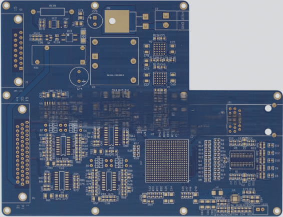
The primary consideration in designing the PCB for a high-speed DSP system is the power supply design. In this context, several methods are typically employed to address signal integrity issues.
1. **Decoupling Power and Ground**
Regardless of whether the circuit board features dedicated ground and power layers, it is essential to incorporate adequately distributed capacitance between the power supply and ground. To optimize space and minimize the number of vias, using more chip capacitors is advisable. These chip capacitors can be placed on the back of the PCB, where the soldering occurs. They should be connected to the vias with wide traces, linking both the power supply and ground.
2. **Power Distribution Wiring Rules**
Separate the analog and digital power planes. High-speed, precision analog components are highly sensitive to digital signals. For instance, amplifiers can inadvertently amplify switching noise, causing it to resemble pulse signals. Consequently, the power layers for the analog and digital sections of the board should be distinctly separated.
3. **Isolating Sensitive Signals**
Certain signals (like high-frequency clocks) are particularly vulnerable to noise interference and require stringent isolation measures. High-frequency clocks (above 20 MHz or with flip times under 5 ns) should be accompanied by a ground trace. The clock trace width must be at least 10 mil, while the ground trace should be no less than 20 mil. Ensure proper contact with ground, connecting it every 5 cm; additionally, a series damping resistor of 22Ω-220Ω should be incorporated on the clock output. These strategies help mitigate interference from signal noise.
4. **Software and Hardware Anti-Jamming Design**
Typically, PCB designs for high-speed DSP applications are tailored by users based on specific system requirements. Given constraints in design capabilities and laboratory conditions, failure to implement effective anti-jamming measures can lead to issues in less-than-ideal environments. Electromagnetic interference (EMI) can disrupt DSP program execution, potentially resulting in program anomalies or even component damage. It’s vital to adopt appropriate anti-jamming strategies.
**1. Hardware Anti-Jamming Design**
Hardware-based anti-jamming is highly effective. When system complexity, cost, and size permit, hardware solutions are preferred. Commonly employed hardware anti-jamming techniques include:
(1) **Hardware Filtering:** RC filters can significantly attenuate various high-frequency interference signals, such as “burr” noise.
(2) **Proper Grounding:** Designing a grounding system is crucial, especially for high-speed digital and analog circuits. A low-impedance, large-area ground layer provides a return path for high-frequency currents, minimizing EMI and RFI while also offering shielding against external interference. During PCB design, keep analog and digital grounds separate.
(3) **Shielding Measures:** Electrical sparks from AC power, high-frequency equipment, and strong currents can generate electromagnetic waves, creating noise sources. Encasing these devices in a grounded metal shell can effectively reduce interference caused by electromagnetic induction.
(4) **Optical Isolation:** Optical isolators are effective in preventing mutual interference between different circuit boards. High-speed optical isolators are frequently used at the DSP interfaces with other devices (e.g., sensors, switches).
**2. Software Anti-Jamming Design**
Software-based anti-jamming offers unique advantages that cannot be replaced by hardware measures. In a DSP application system, it’s crucial to fully leverage software’s anti-jamming capabilities to mitigate interference effects. Some effective software strategies include:
(1) **Digital Filtering:** Digital filters can eliminate noise from analog input signals. Common techniques include median filtering and arithmetic mean filtering.
(2) **Setting Traps:** Reserve a section of boot code in unused program areas. If interference causes the program to jump to this area, the boot code can redirect the captured program to a specified address and use a specialized program to correct any errors.
(3) **Instruction Redundancy:** Insert two or three no-operation (NOP) bytes following double-byte or three-byte instructions to help prevent the program from deviating when the DSP system is disturbed.
(4) **Watchdog Timing:** To recover from an “endless loop,” the watchdog timer technique can be employed. A timer generates a pulse at a set interval; if the DSP does not reset the timer within this period, the pulse serves as a reset signal, reinitializing the DSP.
**3. Electromagnetic Compatibility Design**
Electromagnetic compatibility (EMC) refers to the capacity of electronic equipment to function properly within a complex electromagnetic environment. The goal of EMC design is twofold: to enable devices to suppress external interference and to minimize their own electromagnetic emissions. PCB designs often experience varying degrees of electromagnetic interference, such as crosstalk between adjacent signals. The extent of crosstalk is influenced by the distributed capacitance and inductance of the loops. To mitigate mutual electromagnetic interference, consider the following measures:
1. **Choosing Appropriate Trace Widths**
Transient current-induced interference primarily arises from the inductance of printed traces, which is directly related to their length and inversely related to their width. Thus, using shorter and wider traces is advantageous in suppressing interference. Signal traces for clock leads and bus drivers, which often experience large transient currents, should be minimized in length. For discrete component circuits, trace widths of about 1.5 mm are typically sufficient, while for integrated circuits, widths should range from 0.2 mm to 1.0 mm.
2. **Employing a Grid Wiring Structure**
Adopt a tic-tac-toe wiring structure, with horizontal traces on one PCB layer and vertical traces on the next.
**4. Heat Dissipation Design**
To enhance heat dissipation, it is preferable to install the printed board with a spacing greater than 2 cm. Additionally, observe component layout rules: position high-power devices as close as possible to the PCB edge to shorten heat transfer paths. Vertically, high-power devices should be located near the top of the board to minimize their thermal impact on other components. Sensitive components should be placed in cooler areas and not directly above heat-generating devices.
In the design of high-speed DSP application systems, the transition from theoretical design to practical implementation hinges on the quality of the PCB. Improving signal quality is crucial; thus, the system’s performance is closely linked to the designer’s PCB craftsmanship.
If you have any PCB manufacturing needs, please do not hesitate to contact me.Contact me

