1. Currently, the country has increasingly stringent requirements for environmental protection and greater efforts in link governance. This presents both a challenge and an opportunity for PCB factories. If these factories are committed to addressing environmental pollution, FPC flexible circuit board products can lead the market, providing PCB factories with avenues for further development.
2. The Internet era has disrupted traditional marketing models, gathering a wealth of resources through online platforms, which has significantly accelerated the development of FPC flexible circuit boards. As this pace quickens, environmental issues are likely to arise within PCB factories. However, alongside the growth of the Internet, advancements in environmental protection and environmental informatization have also progressed rapidly. Environmental data centers and green electronic procurement are gradually being integrated into actual production and operations. From this perspective, the environmental challenges faced by PCB factories can be addressed through two main approaches.
1. Emphasize innovation in energy conservation and emission reduction. PCB manufacturers should prioritize Internet technology, integrating comprehensive industry knowledge to enable practical applications of automated monitoring and intelligent management in production processes.
2. Stay attuned to the trends in environmental protection informatization and advancements in various eco-friendly technologies. PCB factories can leverage big data to monitor pollution discharge and treatment outcomes, allowing for timely identification and resolution of environmental issues. Adopting modern production concepts is essential to enhance resource utilization and achieve green production. This will help the PCB industry transition to an efficient, economical, and eco-friendly production model while actively aligning with national environmental policies.
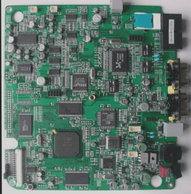
In the PCBA patch processing, multiple stages exist, and the quality at each stage directly influences the final product’s quality; thus, meticulous attention and quality control are essential at every step.
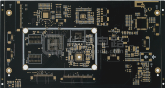
1. PCB Circuit Board
Upon receiving a PCBA patch processing order, the PCBA factory’s initial task is to analyze the Gerber file, taking into account factors such as PCB hole spacing, board load capacity, high-frequency signal interference, and impedance.
2. Component Procurement and Inspection
Component procurement requires ensuring quality through reliable channels, ideally sourcing from reputable distributors and manufacturers. Incoming materials must undergo stringent inspections.
3. SMT Assembly Processing
Key considerations include solder paste printing and reflow oven temperature management. The quality of the laser stencil must meet process specifications, and the steel mesh should be tailored to PCB requirements. Reflow soldering temperature and speed must be precisely controlled, and rigorous AOI testing should be conducted to minimize human error defects.
4. Plug-in Processing
During plug-in processing, the mold design for wave soldering must comply with specified requirements, as effective mold usage enhances the likelihood of producing quality products post-furnace.
5. Program Burning
In the DFM report, it is advisable to recommend that customers incorporate test points on the PCB to verify circuit continuity after soldering components. The customer-provided program can be burned into the main control IC using a burner, allowing for testing of functionality changes due to various touch actions, ultimately verifying the entire PCBA’s function.
6. PCBA Board Testing
For PCBA patch processing, the primary testing components include ICT, FCT, aging tests, temperature and humidity assessments, and drop tests.