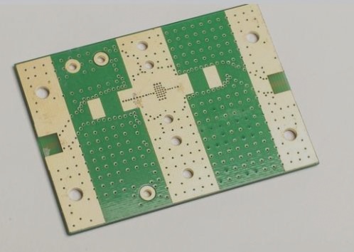
Hello All
I am trying to achieve different trace width for same 50ohm impedance in the same layer in a 6 layer board. My current idea is to refer L1 traces having small thickness(5 mils 50 ohm) to L2 as reference,And for thicker traces (10mils 50ohm) to L3 by giving a keep-out in L2(GND) layer and give a GND polygon on L3 for referring L1 with L3. Is it a feasible solution. Any other ideas are welcome.
Please note that thicker trace are for RF. And i have only very little experience with RF voodoo
L1______________________ ____ ____Top Plain
L2>>>>>>>>>>>>>>>>>>>>> >>> GND Plain
L3…………………………………….. …………. …..SIG1 + GND
L4,,,,,,,,,,,,,,,,,,,,,,,,,,,,,,,,,,,,,,,,,,,,,,,,,,,,,,,,,,,,,,,,,,,SIG2
L5<<<<<<<<<<<<<<<<<<<<<<<<<<<<<<PWR
L6__________________________________Bottom

