**1. Discussing the Experience of PCB Copper Cladding in Circuit Boards**
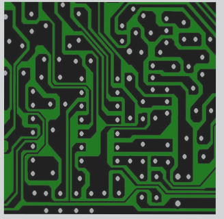
Copper cladding refers to filling the open spaces on a PCB with solid copper. These copper regions are commonly called copper fills. The primary purpose of copper cladding is to reduce ground impedance, enhance the board’s ability to resist interference, decrease voltage drop, improve power supply efficiency, and reduce the loop area by connecting to the ground. When a PCB has multiple pads, such as Sgnd, Agnd, GND, and others, how should copper cladding be applied? My approach is to use the most critical “reference” ground as the basis for independent copper layers, taking into account the varying positions on the PCB. Additionally, I separate digital and analog sections for copper cladding, as appropriate. Along with the copper fill, I ensure that the corresponding power connections—such as V5.0V, V3.6V, V3.3V, etc.—are clearly defined.

**As a result, various deformable structures with different shapes are formed. The copper cladding needs to address several challenges:**
1. **Different single-point connections**: The solution is typically to connect these points using 0-ohm resistors, magnetic beads, or inductance.
2. **The proximity of the crystal to the copper cladding**: The circuit around the crystal is a high-frequency emission source. The practice is to surround the crystal with copper and then ground the shell of the crystal’s vibration through other means.
3. **The island (dead zone) issue**: If the island is large, defining a hole may not be feasible. Large-area copper or mesh-clad copper is generally preferable, but it can be difficult to promote. Why is that? Large-area copper cladding can cause issues during wave soldering, such as board tilting or even blistering. From this perspective, power grid heat dissipation is more efficient. High-frequency circuits typically use this approach to meet the interference suppression requirements of multi-purpose power grids, while low-frequency circuits often have large current flows and are more commonly paired with all-copper circuits.
### **2. Points to Consider When Converting CAD Files to Gerber Files**
**(I) Issues to Watch Out for When Converting from Protel for Windows to Gerber:**
1. **PFW can automatically generate D code tables based on PCB files**, but these tables may contain hundreds of D codes. It’s crucial to understand the capacity of the optical drawing system for D codes.
2. **If PFW does not automatically generate D code tables, errors may arise** due to the following reasons:
– There may be 0 pads or wire sizes in PFW.
– An embossed solder plate may be present.
– D codes may not be configured properly.
In such cases, a large number of D codes may appear in the MAT file.
3. **PFW features long octagonal pads**, which should not be present in the D code table conversion. Since most optical drawing systems do not accept this definition, the presence of such D codes can lead to errors. The best practice is to use the Fill method to match this D code.
4. **It is recommended to use a user-defined D code table** instead of relying on PFW to automatically generate one.
**(II) Issues to Consider When Converting from Protel for DOS to Gerber:**
1. **The upper and lower limits for D code matching should not be too wide**, as this can cause significant deviation and result in an insufficient minimum distance.
2. **Sometimes the filling area (filling) conversion may cause confusion**. In such cases, delete all Chinese-type D codes in the D code table and perform the conversion again.
3. **If D codes do not match and manual matching is required**, be sure to select Mode 3.
4. **In arc (ARC) conversions**, do not set the step distance (arc quality) too small, as it may generate excessive data and produce jagged arc edges.
5. **Resistance welding expansion values can be negative**.
6. **In ARC conversion**, you can choose between arc descriptions or straight-line descriptions:
– **Software Arc: On**: This is described by a straight line, and during conversion, the polyline approximates a circular arc.
– **Software Arc: Closing**: This describes a true arc. It’s best to use an optical plotter that accepts arc descriptions, as this minimizes data size and ensures smooth edges for light-drawing arcs.
7. **If the D code used exceeds 24**, the G54 option must be enabled.
8. **When a single-sided pad needs to be punched**, ensure the “Pad Holes” option is enabled under Options > Single Layer.
9. **Certain tool software** can generate a fully configured D code table via the MAT file.
**(C) Considerations When Transferring Gerber Files from PowerPCB:**
1. **After conversion, PowerPCB files may require copper filling**.
2. **Since PowerPCB is a Windows-based software**, the MAT file is largely similar during file conversion. It’s essential to verify the selected elements in each drawing to avoid errors due to incorrect graphic transfers.
**(IV) Considerations When Transferring Gerber Files from PADS:**
1. **PADS’ preset D code table may have insufficient capacity**, requiring an expansion of its limits.
2. **After conversion, a gasket file may need to be filled with copper**.
3. **Due to the specific design structure of pads in PADS**, it is important to ensure that the correct elements are selected in each drawing to prevent errors from incorrect graphic transfers.


