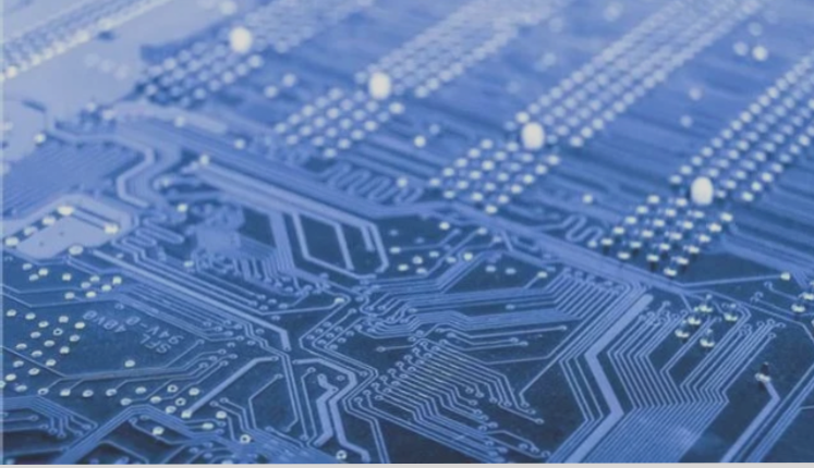
PCB (Printed Circuit Board) Design and Assembly Process
A Printed Circuit Board (PCB) efficiently integrates electronic components, optimizing space and ensuring seamless circuit operation. The PCBA assembly facility plays a vital role in supporting electronic components and establishing circuit connections.
Key Steps in PCB Design:
- Access the PCB design system and configure relevant parameters, such as grid size and layer specifications.
- Generate the netlist, a crucial link between circuit schematic design and PCB layout.
- Arrange component placement using automatic layout features and manual adjustments as needed.
- Perform PCB wiring with attention to parameters like safe distances and wire types.
- Output the final PCB schematic file via printer or other graphic output devices.
Advancements in PCB Technology:
PCBs, known for their “printed” manufacturing process, benefit from Surface Mount Technology (SMT), resulting in high assembly density, reduced size, and lighter electronic products. SMT can decrease product volume by 40% to 60% and weight by 60% to 80%. While automatic wiring functions are advanced, manual routing may still be necessary for optimal line layout.