Importance of Screen Printing on Printed Circuit Boards
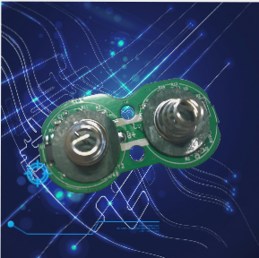
Printed circuit boards play a vital role in electronic circuits, powering devices through compact chips. As technology advances, PCBs have shrunk in size while accommodating numerous components for connections and information transmission.
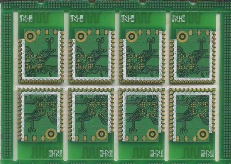
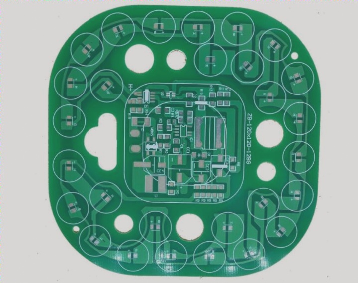
One key aspect of PCB manufacturing is the application of screen printing. The silk screen layer on a PCB consists of ink traces that help identify components, marks, logos, and symbols. Originally used on the component side, silk screen printing is now common on the soldering side as well.
Screen printing simplifies the identification of different parts, aiding manufacturers and engineers in assembly and troubleshooting processes.
Advancements in PCB Technology
- Miniaturization of PCBs due to technological progress.
- Integration of multiple components in a small area.
- Enhanced information transmission capabilities.
Future of PCBs
With ongoing innovations, PCBs are expected to become even smaller and more efficient, driving the development of compact and powerful electronic devices.


