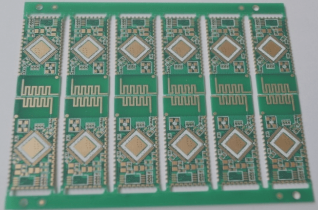
PCB Wiring Tips and Best Practices
Features:
- The orientation of components determines the direction of PCB wiring.
- Adjacent layers have different wiring directions.
- Rectangular PCBs should have vertical wiring to avoid congestion.
- Ensure sufficient wiring space to prevent circuit failure.
Analog and Digital Circuit Separation:
Keep analog and digital sections at least 5mm apart to prevent signal interference. Design power and ground lines first for optimal electrical performance and noise immunity.
Example: Two-layer PCB

- Power and ground lines on the same layer result in poor performance.
- Separate ground and power lines on different layers for better noise immunity.
- Consider wider trace width for better current flow and heat dissipation.
- Use large copper foil routing for power and ground lines.
Key Considerations for PCB Design:
- Surround critical components with ground copper foil to reduce interference.
- Use thermal pads for heat dissipation during soldering.
- Utilize thermal resistance pads to manage heat dissipation effectively.
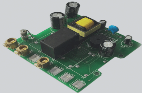
Introduction to PCB Layout and Design, Power Supply for Analog Circuits
Best Practices for PCB Layout
The placement of the output section near the power supply and the high-sensitivity input section away from the output is crucial to avoid interference.
Schematic of Analog Circuit and Power Supply Separation
For the DC power supply, external power should first go through an electrolytic capacitor before reaching the internal circuit. In a two-layer PCB, route the power via point B instead of point A. In a multi-layer PCB, bring the power to an inner layer after passing through point B.
If you require PCB manufacturing services, feel free to contact us.