PCB Design for Switching Power Supplies
In the realm of switching power supply design, the PCB’s physical design stands as the final crucial step. A flawed design approach can result in excessive electromagnetic interference, leading to operational instability in the power supply. Let’s delve into the process:
Design Process Overview:
- Commence with component parameters from the schematic and transition to PCB design flow.
- Input the principal netlist, set design parameters, perform manual layout and routing.
- Verify the design, conduct a thorough review, and proceed to CAM output.
Parameter Settings:
When setting parameters, ensure that the distance between adjacent traces adheres to electrical safety standards. For ease of handling and production, maximize this distance. The minimum spacing should meet voltage withstand requirements. In instances of low wiring density, adjust the spacing for signal lines accordingly, with a recommended trace spacing of 8 mils.
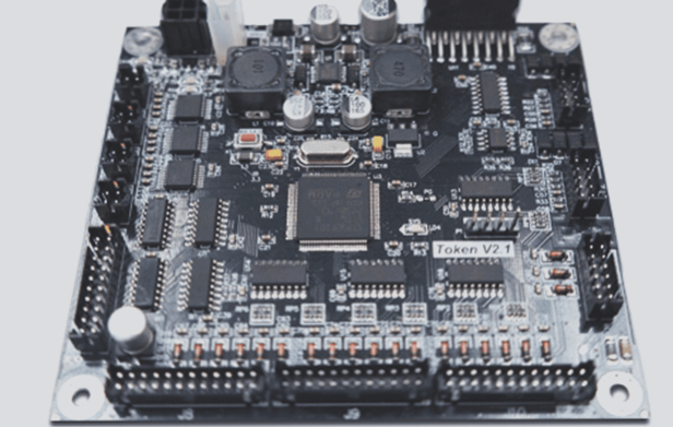
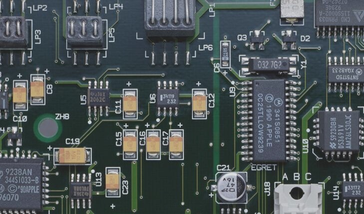
Proper Component Layout:
Experience has shown that even with a correct schematic design, improper PCB design can jeopardize electronic equipment reliability. For instance, closely spaced thin parallel lines may lead to signal delays and noise reflection. Adequate consideration of power supply and ground is essential to avoid performance degradation. Correct methods in PCB design are crucial, with each switching power supply comprising four current loops:
- Power switch AC circuit
- Output rectifier AC circuit
- Input signal source current loop
- Input circuit of the output load current loop
Optimal Layout Sequence:
The layout sequence mirrors the electrical design:
- Place the transformer
- Design the power switch current loop
- Design the output rectifier current loop
- Connect the control circuit to the AC power circuit
- Design the input current source loop and filter
- Design the output load loop and filter
Component Placement Principles:
- Consider PCB size to avoid impedance issues and reduce costs.
- Ensure components are not densely arranged to facilitate future soldering.
PCB Layout Best Practices
When designing a PCB layout, it is crucial to consider the following guidelines:
- Utilize the core component of each functional circuit as the central point for layout to ensure components are evenly and neatly arranged.
- Minimize lead length and connections, and place decoupling capacitors close to the VCC for optimal performance.
- For high-frequency circuits, take into account distributed parameters between components and arrange the circuit in parallel for improved aesthetics and ease of installation.
- Position functional circuit units according to the circuit flow to enable convenient signal circulation with consistent signal direction.
- Focus on routing efficiency by avoiding flying line connections and grouping interconnected devices together.
- Reduce loop area to minimize radiation interference from the switching power supply.
Latest PCB Design Trends
With the advancement of technology, PCB design trends are constantly evolving. Some of the latest trends include:
- Integration of IoT capabilities into PCBs for enhanced connectivity.
- Increased use of flexible and rigid-flex PCBs for space-saving and design flexibility.
- Implementation of advanced thermal management techniques to improve overall performance.
- Adoption of high-speed design practices to meet the demands of modern electronics.
- Utilization of advanced simulation tools for accurate signal integrity analysis.