FPGA Pin Assignment Verification
When designing a PCB with FPGA devices, verifying pin assignments early using Quartus II software is crucial. This step ensures correct pin configuration before schematic design, preventing issues in later stages.
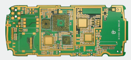
Layer Stackup for Multilayer PCBs
Layer stackup is vital in PCB design, especially for multilayer boards. For a 4-layer PCB, the order is top signal plane, ground plane, power plane, and bottom signal plane. For a 6-layer PCB, the stackup includes top signal plane, ground plane, two inner signal layers, power plane, and bottom signal plane. More layers offer improved EMI shielding.
Power Distribution in Multi-Voltage Systems
Designing power distribution for complex systems like FPGA + DSP requires multiple voltage rails. A typical 6-layer PCB may include 3.3V (main supply), 1.2V and 1.8V (core supplies), and 5V (input power). Careful routing, avoiding wire connections, and using copper pours for low resistance paths are essential for stable power distribution.
Power Supply Network and Copper Pour
In PCB design, using copper pour for power planes simplifies routing, reduces resistance, and minimizes noise issues, improving overall performance by shortening trace lengths.
Layer-to-Layer Routing: Cross-Hatching Method
For multi-layer PCBs, cross-hatching routing minimizes EMI between traces, reducing signal degradation and optimizing space efficiency on each layer.
Analog and Digital Isolation
Proper isolation between analog and digital circuits involves separating components on the layout, using dedicated analog grounds, and connecting analog power to digital supply at a single point to prevent interference.
Iterative Approach in PCB Design (Using Design Software)

PCB Design Best Practices
PCB design shares similarities with software development, focusing on iterative processes to minimize errors. Key steps include:
-
Schematic Verification
Double-check the schematic, paying close attention to power and ground connections.
-
PCB Package Review
Ensure component pin assignments are accurate and match the schematic.
-
Package Size Verification
Confirm package sizes and label components for easy reference.
-
Netlist Importation and Signal Adjustments
Import the netlist, make necessary schematic adjustments during layout, and avoid automatic numbering functions.
-
Manual Routing
Continuously check power and ground networks, use copper pours for efficient signal paths.
The success of PCB design lies in continuous feedback and correction, focusing on signal integrity and routing efficiency.
Crystal Oscillator Placement Tips
Place the crystal oscillator close to the driven chip, shield it with a dedicated ground plane to reduce noise, and use a tree-shaped clock distribution network for multiple components.
Connector Signal Arrangement Importance
Signal arrangement on connectors impacts PCB routing complexity. Plan signal order early, and avoid renumbering components post-layout to minimize errors.
Multi-Board Connector Design Considerations
-
Flat Cable Connection
Ensure identical upper and lower interfaces for flat cable connections.
-
Straight Socket Design
Mirror and symmetrical interfaces for straightforward socket connections.
Module Connection Signals Strategies
-
Same-Side Module Placement
Connect control signals to the smaller module using a mirror connection scheme.
-
Opposite-Side Module Placement
Connect control signals to both smaller and larger modules for signal integrity.